
How Humans Learned to Boss Electrons Around
In 1883, Edison was still fighting with his light bulb. The filament was carbon back then, and carbon doesn't last — heat it enough to glow and it evaporates. The evaporated carbon coated the inside of the glass and blackened the bulb, so he stuck a metal plate in next to the filament, hoping to catch it. The bulb still went black. But Edison noticed something odd: when the lamp lit up, a faint current appeared in that metal plate, even though it never touched the filament.
He had no idea what it was good for. But out of pure inventor's reflex, he patented it anyway and called it the Edison effect.
What Edison didn't realize is that this pointless little current was the first time a human watched themselves steer electrons. Everything that followed — the vacuum tube, the transistor, the chips with a hundred billion switches in them — grew out of that metal plate.
Heat a filament red-hot and the electrons get restless
When the filament glows, the electrons inside it get energetic enough to fly off in all directions. Physicists call it thermionic emission. Some of those escaping electrons land on the nearby metal plate, and that's the faint current Edison saw.
The breakthrough move is to wire that metal plate up as an electrode you can put a positive charge on. Electrons are drawn to positive charge, so they pour across and the current grows. Flip that electrode negative and the electrons turn around — the circuit goes open.
One side that emits electrons (the cathode), one side that receives them (the anode), and current that flows in only one direction: that's a diode. Its signature trick is turning alternating current into direct current. Current in the right direction passes; the wrong direction gets blocked; wire four of them into a bridge and the back-and-forth of AC gets flattened into smooth DC. That's roughly what the charger on your desk is doing.
Add a wire mesh and a weak signal can command a strong one
Now slide a metal mesh in between the cathode and the anode and put a voltage on it, so the mesh carries an electric field. Every electron flying from cathode to anode now has to get past that mesh: a stronger field on the mesh blocks more of them, a weaker field lets more through.
That mesh is the grid, and a tube with a grid is a triode. The beautiful part is that a tiny nudge in the grid's voltage swings the number of electrons getting through by a lot — so a weak signal can control a strong current. Put another way, a faint signal comes out amplified. There's still a crowd of audiophiles building tube amps off exactly this trick today. (Redknot, whose videos this series is built from, admits he can't actually hear the difference.)
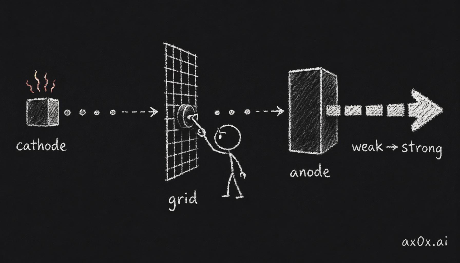 In a triode a tiny change in the grid's voltage swings how many electrons get through — a weak signal becomes an amplified strong current.
But the tube's flaws are glaring. The filament has to be heated red-hot, so it runs hot and burns power; it needs three to ten seconds to warm up before it works; and to keep the filament from oxidizing in air, the whole thing lives inside a vacuum-sealed glass shell. None of that shrinks. The tube has mostly vanished from daily life — it survives in the magnetron in your microwave and the X-ray emitter in a CT scanner, and not many places else.
You don't need a glowing filament to control electrons
Heating a filament is a clumsy way to do this. Time for a different idea, and the star is silicon.
A silicon atom has four electrons in its outer shell, each holding hands with a neighboring silicon atom to form a covalent bond, and that locks the electrons down tight — so pure silicon doesn't actually conduct. To make it conduct, you mix something else in. This is called doping. Add a little phosphorus (five outer electrons) and there's one electron left over with nowhere to bond; it becomes a free electron, and this silicon now conducts via negatively charged electrons — call it N-type. Add a little boron (three outer electrons) and now you're one short; that leaves a "hole," and this silicon conducts via positively charged holes — call it P-type.
Take one slab of silicon, dope half of it N-type and half P-type, and the border between them does something interesting. The N side has a high concentration of electrons, so they diffuse over into the P side; but as electrons leave, the imbalance builds an internal electric field that pulls them back. Push and pull settle into a standoff, and that standoff region is the PN junction.
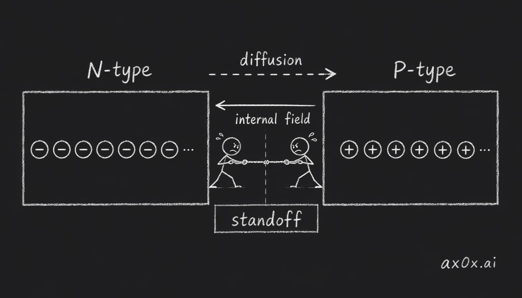 Electrons diffuse from N-type to P-type, and the resulting internal field pulls them back — push and pull settle into the PN junction's standoff.
A PN junction conducts in one direction only: current flows when the external voltage points the right way and is strong enough (usually over 0.7 volts) to cancel that internal field; point it the wrong way and the junction clamps itself shut even harder. So a doped slab of silicon, with no glowing filament anywhere, recreates the diode. As a bonus, a PN junction is sensitive to light too — shine light on it and it produces current, which is exactly how a solar panel works.
What if you crank the voltage way up? The racing electrons start knocking other electrons out of their covalent bonds, and those knocked-loose electrons knock out more — it snowballs. As Redknot puts it, it's like the chain reaction inside an atomic bomb. This is avalanche breakdown; it doesn't wreck the device by itself, but it dumps a lot of heat, and if you can't shed it the silicon burns through.
Bolt a switch onto the PN junction and you get the modern transistor
A diode only passes current one way, which still isn't enough. The thing that actually rewrote everything is a controllable switch.
Take a slab of silicon and dope two N-type regions — a source and a drain — with a stretch of P-type between them. Normally the PN junctions wall the two N regions off, so no current flows. Now, over that middle P stretch, separated by a thin insulating film, add an electrode (the gate). Put a positive voltage on the gate and it pulls a field downward, dragging electrons up to the top of the P region and forcing a conductive "N-channel" into existence — the two N regions are suddenly connected. Drop the voltage and the channel collapses; open again.
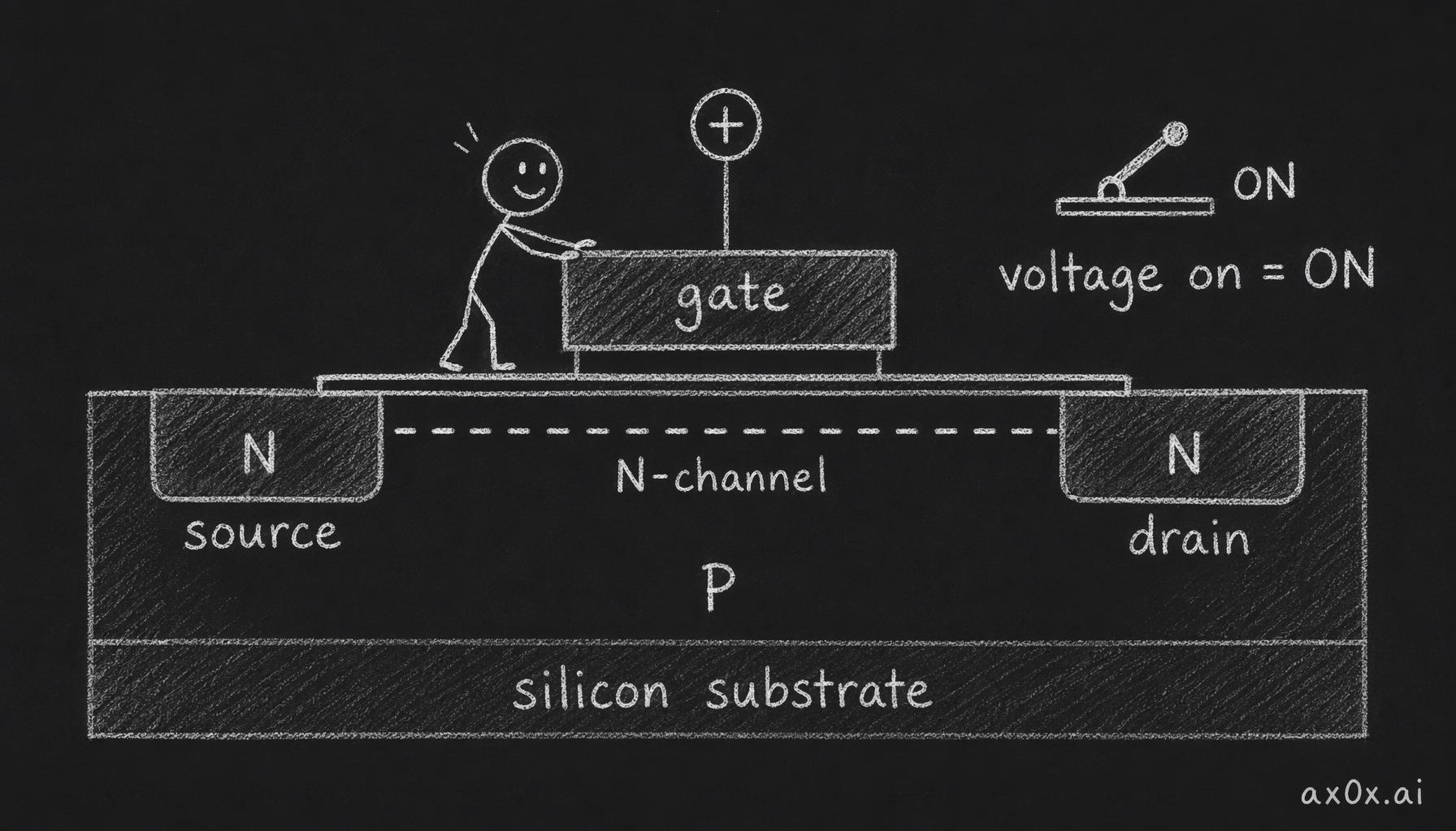 A positive voltage on the MOSFET gate forces an N-channel that connects source and drain; drop the voltage and it opens — a controllable switch.
This is the MOSFET — metal-oxide-semiconductor field-effect transistor. The name is intimidating until you unpack it: metal is that gate electrode, oxide is the insulating film under the gate (silicon dioxide), and semiconductor is the doped silicon underneath. When an ad brags that some chip "integrates a hundred billion transistors," it means a hundred billion of these little switches are packed onto a slab of silicon the size of your palm.
Against the tube, it doesn't need heating, doesn't need warm-up, doesn't fear oxidation, and shrinks to the nanometer scale — the vacuum tube lost cleanly. From a metal plate that accidentally carried a current, to a sliver of silicon holding a trillion switches, it took humans the better part of a century to get electrons fully in hand.
But a pile of switches still can't do arithmetic. How these switches get wired into a CPU that remembers and computes is the next post. And how these nanometer-scale things get drawn onto silicon in the first place is the lithography post that closes this series.
This series is compiled from the hardware-explainer videos of Bilibili creator Redknot-乔红. He explains this stuff with far more detail and far better jokes than I've kept here — the originals are well worth watching. I've only reorganized it by theme and written it up; any errors are mine, not his.