
Taming Light Inside a Chip
Redknot floats a bold claim in one of his videos: what really marks the height of a civilization is the grandest engineering it can build by commanding the forces of nature. I'm inclined to agree. And the lithography machine that prints chips is about the most representative piece of engineering our era has.
The transistors, caches, floating gates, and capacitors from the first four posts are all, in the end, microscopic structures on slabs of silicon. How do they get drawn on? With light. And the same thing — light — turns around and builds screens. This post is about how humans tamed light into both a chisel and a paintbrush.
Lithography: drawing circuits onto silicon with light
The flow isn't complicated: print the circuit pattern onto a template called a mask, shine light through the mask onto a wafer coated in photoresist, the lit resist changes and rinses away in developer, the exposed wafer goes to etching, and the mask's pattern is now on the silicon.
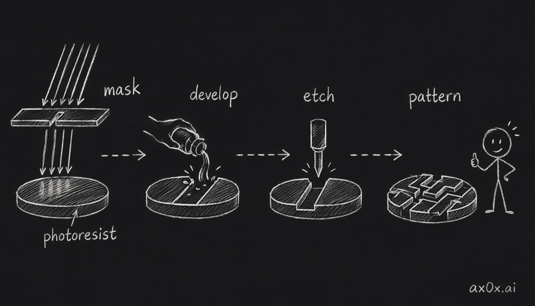 The five-step lithography flow: light through a mask hits photoresist, developer rinses the changed resist, etching follows, and the circuit pattern lands on the silicon.
But once the process shrinks to the nanometer scale, you can't dodge light's quirks anymore. Light is a wave — Thomas Young's double-slit experiment in 1801 nailed that down. And a wave diffracts: light through a narrow slit in the mask doesn't travel in a tidy straight line, it fans out to the sides, and the narrower the slit, the wider it ends up projected on the wafer. That's the bind — you want it fine, and it smears it out.
There are two ways to fight diffraction, which split into two schools. One is to keep the wafer right up against the mask and expose before the light spreads — proximity lithography. The other is to back the wafer off and put a convex lens in between to shrink the mask's pattern down onto the wafer — projection lithography. Projection has one more key figure of merit, the numerical aperture (NA). A bigger lens gathers more of the diffracted light, makes a sharper image, and prints a better circuit. But either way, the most fundamental move to suppress diffraction is to shorten the wavelength. Shorter wavelength, less spread.
X-rays: a brilliant idea that hit a dead end
If shorter is better, go all the way. The first candidate was the X-ray, at about 1 nanometer, and IBM poured effort into it as early as the 1960s; by the eighties and nineties it could actually make chips. Then the X-ray's temper showed.
X-rays are too headstrong. Passing through a body, they barrel straight ahead, almost never bending for any tissue — either through or absorbed — which is exactly why they image us so well, and also why they utterly ignore a glass lens. No lens means no projection, which forces you back to proximity, and proximity is a mess: the mask has to be 1:1 with the chip, so to print 10 nanometers you machine 10-nanometer precision into the mask, which is brutally hard; the wafer hugs the mask at ten to twenty microns, exposing in the very unstable "near-field diffraction" zone where a one-micron gap change scrambles the pattern; and worst of all, to block the X-rays, the mask pattern is made of gold, which absorbs the X-rays, turns them to heat, expands and contracts over and over, and eventually cracks the gold film and ruins the whole mask.
There's a famous scene here. Back at IBM, deep-ultraviolet believer Burn-Jeng Lin (林本坚) — skeptical of X-rays — watched the X-ray team hit a milestone and get celebratory T-shirts from their boss reading "X Ray works." Lin turned his around and wrote three words on the back for passing colleagues to see: "X Ray works for the dentists." History proved his instinct uncomfortably right.
X-rays were ultimately abandoned, and wavelength marched down the projection path instead: 436, 248, 193 nanometers, a failed attempt at 157 (beaten by Lin's 193-nanometer immersion lithography), until humans leapt straight to 13.5 nanometers — extreme ultraviolet (EUV). Why 13.5 exactly? Because go any shorter and again no instrument can steer it. It can't use a glass lens; it relies on a Bragg mirror built from dozens of alternating molybdenum and silicon layers, reflecting about 70% of 13.5-nanometer light. There's actually a molybdenum-beryllium mirror that reflects 11 nanometers with even higher efficiency, but beryllium is severely toxic and no one would dare work in the fab, so to spare our fragile bodies they settled on 13.5. As for going below to 6.7 nanometers, Redknot is pessimistic — he even suspects silicon-based scaling has a real ceiling. He also dearly hopes to be proven wrong.
The same light builds screens: quantum dots
Light can carve chips, and with a twist it can glow. An electron sits at one of several "energy levels" in an atom; inject energy and it jumps to a higher level, and when it falls back the energy difference comes out as light — the bigger the gap, the bluer the light. The catch: in a big crystal, electrons roam across the whole thing, the once-distinct energy levels shatter into a near-continuous smear, and a falling electron doesn't drop in one leap but shuffles down a dense staircase, turning the energy into heat. So shine light on a big crystal and it just warms up, no glow. Redknot has a perfect image for this: a strongman hurls you onto a 20-story rooftop; jump straight down and you'd flash into light; take the stairs and all you get is a sweat.
So what if you shrink the crystal to a few nanometers? The electron gets re-confined to a tight space, the levels snap back to discrete, and a jump-and-fall glows again. Better still, the smaller the crystal the wider the gaps and the bluer the light, the bigger the redder — control the size and you point at a color. This is the quantum dot, the 2023 Nobel Prize in Chemistry. High-end LCD TVs now hit quantum dots with high-energy blue light: smaller dots emit green, larger ones red, and mixed with the original blue you get clean, bright white backlight — far purer than the old phosphor approach.
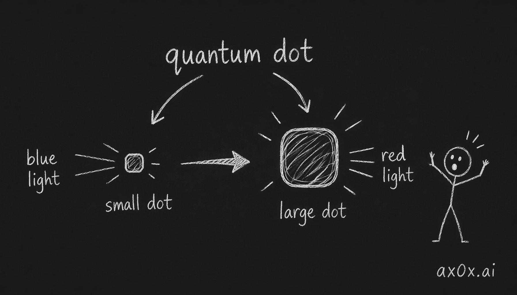 A quantum dot's size sets its color: smaller crystals emit bluer light, larger crystals emit redder light, so tuning size tunes the color.
Then you trap light inside an eyeglass arm: AR waveguides
The display thread gets wilder still. The plain version first: a screen too close to focus on gets a convex lens to enlarge and push its virtual image out to a focusable distance — two screens blocking your whole view is VR; seeing both the screen and the world is AR.
The first way to do AR is called birdbath: a screen sits up top and a half-mirror spherical surface folds the image into your eye, named because that spherical mirror looks like the basin in a public park where birds bathe. It's bright but thick and dim, no good as everyday glasses. To go slim, you tuck the screen into the temple arm and use a glass's total internal reflection to pipe light to your eye and release it. But waveguides immediately slam into AR's "impossible triangle": field of view (FOV, how much of your vision the image fills), eye box (how far your eye can roam and still see the full image), and lens size — push one and the others give. A lens stuffed in the temple can't be big, so a bigger FOV costs you eye box, and one twitch of the eye and you see nothing. Engineers fix it by opening several exit points to give the eye room, either via stacked half-mirrors (geometric array) or grating diffraction (diffractive waveguide). But diffraction has a pitfall: different colors diffract at different angles, so RGB comes out the waveguide misaligned, the image beaten black and blue — which is why plenty of diffractive-waveguide glasses just go single-color green, since aligning three colors is hard and the eye is most sensitive to green anyway. To do color, and to stay readable under bright sun, you need a brutally bright Micro LED screen muscling its light against the daylight.
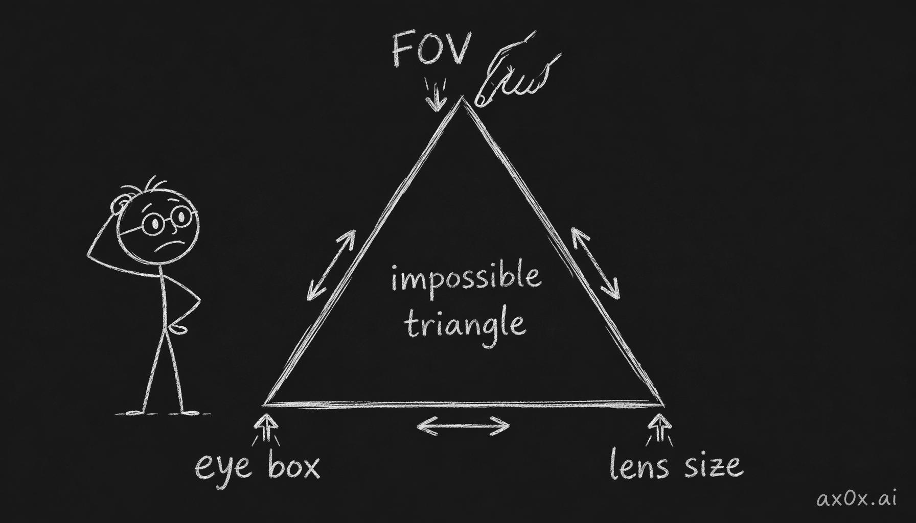 AR waveguides face an impossible triangle: field of view, eye box, and lens size all pull against each other — press one and the others pop up.
Closing
From a glowing filament to a transistor that steers electrons; from a circuit that remembers to a cache that decides performance; from spinning platters and flash to HBM; finally to a machine that embroiders on silicon with 13.5-nanometer light. The whole arc is the same single act: taking electricity and light — the two most unruly forces — and pressing them, bit by bit, into the palm of the hand.
It's just that the silicon road may really have an end. Redknot is pessimistic; I'd happily bet on him being wrong — for a hundred years now, every time someone said "this is the limit," someone else insisted on pushing one inch further.
This series ends here, all five parts compiled from the hardware-explainer videos of Bilibili creator Redknot-乔红. The "strongman throwing you off a 20-story roof" and "X Ray works for the dentists" bits are his — he explains the hard parts with more accuracy and more wit than I've kept. The originals are well worth your time. I've only reorganized by theme and written it up; any mistakes are mine.