The Packaging War — How Close to the Chip Should Light Go
In March this year Broadcom put out a press release saying Tomahawk 6, its 102.4T switch chip, was shipping in production volume. One variant of that chip, Davisson, has the optical engines packaged right next to the switch die — the industry calls this CPO, co-packaged optics. NVIDIA is on the same road: Quantum-X Photonics started shipping early in the year, and Spectrum-X Photonics was declared in full production in August. Both are CPO. Everyone seems to agree CPO is the next generation. What I wanted to know is what problem it is actually solving, and compared with the module plugged into the switch faceplate today, where exactly the savings come from.
The last post followed the light-versus-copper boundary from the ocean floor to the gap between racks over fifty years. This one goes inside the rack, and inside the chip package.
The expensive part is the last twenty or thirty centimeters
The fiber leg is close to free. A glass strand runs tens of kilometers and the cost barely moves with distance — that was part two. So none of the advanced-packaging schemes, CPO or NPO or the rest, is about the fiber. All of them are working on the electrical path between the chip and the optical engine: the last twenty or thirty centimeters.
Why is that short hop so costly? Part two did the arithmetic: a 224G link can lose on the order of 40 dB across the whole electrical path, and the receiver burns power to recover the signal. Burned power turns into heat, and heat costs power again — the figure given on the show was that equipment and cooling split a data center's electricity bill roughly in half, so every extra watt inside a module is paid for more than once. That's how twenty or thirty centimeters of copper trace ended up as the most expensive segment of the entire link, while the kilometers of fiber next to it are the cheapest.
The most expensive, hungriest chip in the module
In part one I took apart an 800G module and skipped past the DSP in the middle of the signal chain. It needs its own section, because the packaging war is really a fight over this one chip. Inside an optical module it's called the ODSP, optical DSP; Kevin calls it the module's brain. Its job list runs roughly like this: it does the SerDes receive-and-transmit work and the equalization, cleaning up the electrical signal that has been bounced across the PCB; it compensates for what the optical channel does to the signal — bandwidth limits, dispersion, nonlinearity; and it runs the FEC error correction. Anything that got distorted and needs to be reconstructed lands on the ODSP.
It is also where the power goes. Roughly half a module's power draw is that one chip. Kevin walked through the budget on the episode: an 800G module has to stay under 16 W, so the DSP itself has to come in under 8 W, and since the DSP handles 8 lanes, each lane gets less than 1 W. At 1.6T the whole module pushes toward 25 W, at a moment when data centers can't find a spare watt anywhere.
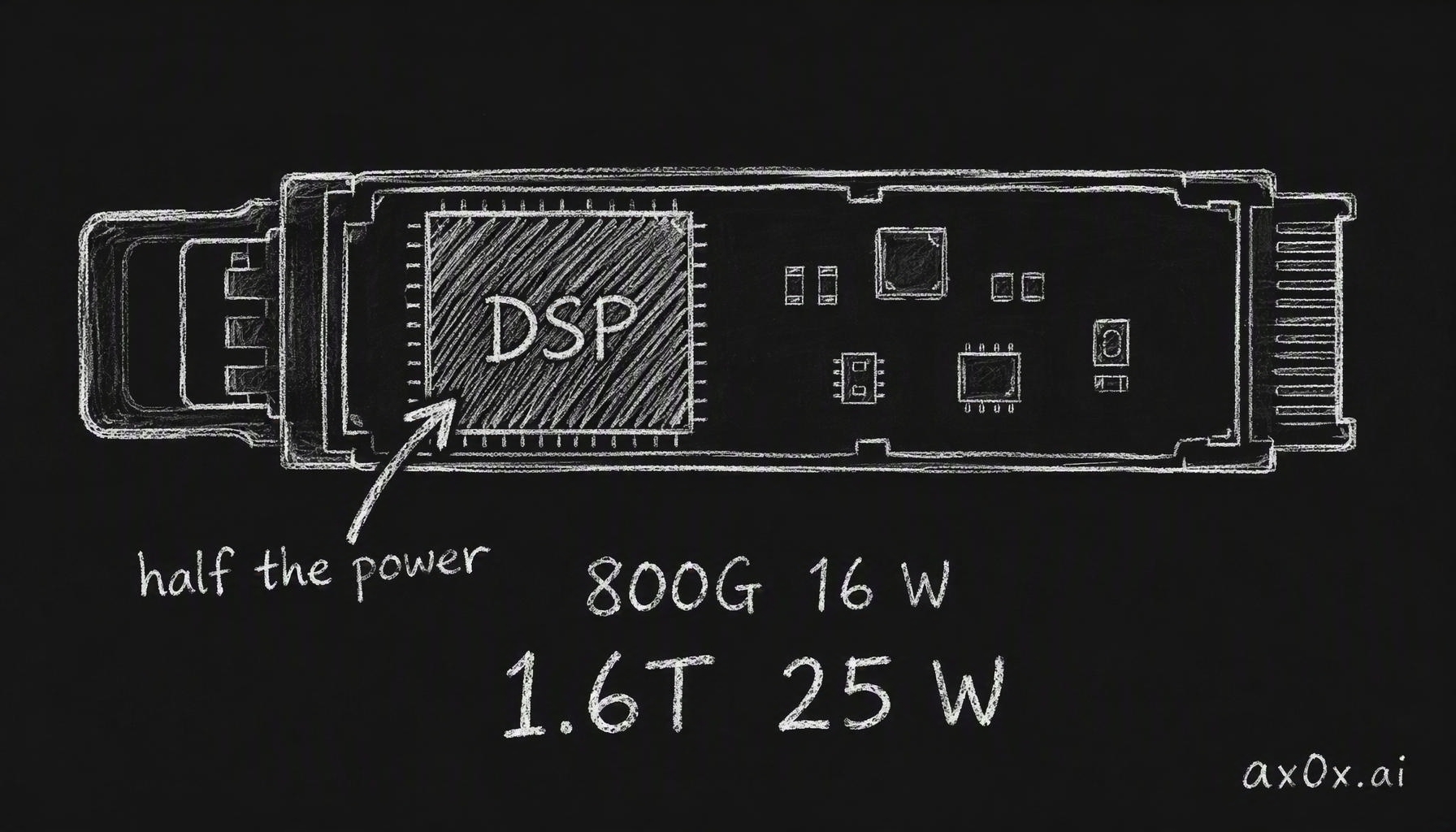 The DSP inside an optical module is its brain and its biggest power hog — roughly half the module's watts go to it: about 16 W for 800G, close to 25 W for 1.6T
What makes this chip hard? Kevin gave three reasons. First, the analog performance is at the edge of what's possible: 224G per lane puts the Nyquist frequency around 56 GHz, which calls for fast, high-precision ADCs, an analog front end with bandwidth on the order of 55–60 GHz or more, and sampling-clock jitter on the order of tens of femtoseconds RMS, up to about a hundred — and all of that mixed-signal design has to be done on 5 nm or 3 nm process nodes. Only a handful of teams in the world can do it. Second, the trade-off between algorithm and power: stronger equalization recovers the signal better and blows through the budget, which is exactly how that 1 W per lane gets pinned. Third, the price of entry: one tape-out on an advanced node runs to tens of millions of dollars, on top of years of accumulated SerDes IP, co-simulation of the optical and electrical sides, and the ability to test at volume.
So the market is concentrated. ODSPs come mostly from Marvell and Broadcom, with Marvell clearly ahead and Broadcom chasing, and Credo holding a slice. Kevin mentioned in passing how Broadcom got there: it bought company after company over more than twenty years. That moat was stacked up by decades of acquisitions, which is where part five picks up when it looks at who is trying to catch up.
Think of it as a courier network
Back to the question: where does the electrical-to-optical conversion belong? Kevin used a courier-network analogy on the episode that strings every packaging scheme onto one line. He explained it well, so I'm borrowing it whole.
Fiber is the trunk railway: freight costs almost nothing extra per kilometer. The switch chip or GPU is a giant office tower whose parcel volume doubles every two years. The electrical signal is the delivery rider, and the PCB is the street — potholed, with electromagnetic interference thrown in. The awkward part is that each time a parcel goes up a size, meaning each time the data rate doubles, the delivery fee on that same street doubles too. The electrical-to-optical conversion point is the courier depot.
Set it up that way and every packaging scheme becomes one siting decision: how close to the office tower do you build the depot? Far away and the street leg is expensive, but the locker is a standard part you swap out when it breaks. Close in and the street leg is cheap, but now the depot is bolted to the building, and fixing it means opening the building up.
Five places to put the depot
The first is the pluggable module, the one you see today in the faceplate slots of a switch. It's the standard parcel locker outside the building: the slot dimensions are the same nationwide, any vendor's locker fits, and a broken one gets pulled and replaced. The price is that the electrical signal has to travel all the way from the switch die to the faceplate, so the chip needs its strongest-driving, most power-hungry long-reach SerDes, somewhere around 4.5–6 picojoules per bit. And once the signal arrives at the module it gets rebuilt from scratch — that's the ODSP scrubbing it back into shape.
The second is LPO, linear pluggable optics. The module stays in the faceplate; what changes is inside it. The ODSP comes out and a linear driver goes in, so the signal is shaped once at the transmitter and never reconstructed along the way. Module power drops 40–50% — a 16–17 W DSP-based module becomes something like 7.5–9 W as LPO — and latency comes down with it. Sounds great, and then the constraints show up. The PCB link and the SerDes on the switch side now have to be very clean, and when a signal arrives damaged nobody can say whether it was hurt on the board or on the fiber. Mix one vendor's NIC with another vendor's module and each side points at the other, which is the interoperability problem in one sentence. There's a system-level cost too, and Kevin had a rocket analogy for it: drop a stage and the remaining stage has to carry more fuel. If the module no longer recovers the signal, the switch chip has to drive the whole path itself; a switch chip with, say, 512 SerDes lanes that could have used weaker, lower-power drivers now needs all 512 upgraded to stronger, hotter ones, and the whole box's power, cooling and cost move with it. So LPO fits short, clean links, and as of 2026 it hasn't spread far in the 800G generation. The industry is warmer on a halfway form called LRO, which strips out only part of the DSP's functions and lands at roughly 8.5–12 W.
The third is NPO, near-packaged optics. The optical engine goes on the same board as the main chip, and the real electrical path shrinks from tens of centimeters to a few. In courier terms, the street goes from several hundred meters or a kilometer down to a few dozen meters. The switch chip can get by with a short-reach XSR-class SerDes at 1–2 picojoules per bit, several times cheaper than long-reach. The engine is semi-custom but still replaceable as a unit. It's a middle rung between pluggable and CPO, and it's understood as a transition.
The fourth is CPO, co-packaged optics. The locker goes away and the depot moves inside the building, on the same floor as the recipient: the optical engine shares a package substrate with the main chip, and the electrical path is down to millimeters. Long-reach SerDes and the ODSP are mostly gone, so the energy drops a lot. Broadcom claims the previous-generation Bailly CPO runs about 5.5 W per 800G link, against about 14 W for pluggable in its own materials (third-party write-ups say 15 W), and for Davisson it reports around 3.5 W; NVIDIA claims roughly 3.5x better energy efficiency. Both numbers are the vendors' own, with no independent measurement behind them. Two costs come with that, and both are steep. The optical path is now sealed into the package. Lasers age and fibers fail; with a pluggable you pull the dead module and push in a new one, but with CPO the light path is soldered into the package, so when one channel dies only the people who designed it know how to fix it. No hot swap, and maintenance is the real pain. Then there's heat. The optics share a package with a main chip that draws hundreds of watts — Kevin's figure was 700 W — and heat is the one thing lasers hate most.
Further out there's a fifth, OIO, optical I/O, the optical chiplet. Light enters the package directly, right up against the compute die, so even the few millimeters of substrate are gone. Kevin's summary at this point was that the closer the conversion sits to the chip, the more power you save and the harder it is to repair, and the packaging war is the search for the profitable spot between those two ends. One distinction matters here: CPO is a switch-side story serving the scale-out network — Broadcom's Tomahawk and NVIDIA's Quantum-X belong to it — while OIO lives inside and between GPU packages and serves scale-up, where Ayar Labs and Marvell are working. And since TSMC's COUPE silicon photonics platform reached volume production in April, integrated silicon photonics is no longer something only Broadcom and NVIDIA can do. GPU-to-GPU interconnect is the next war and I'm leaving it out of this post.
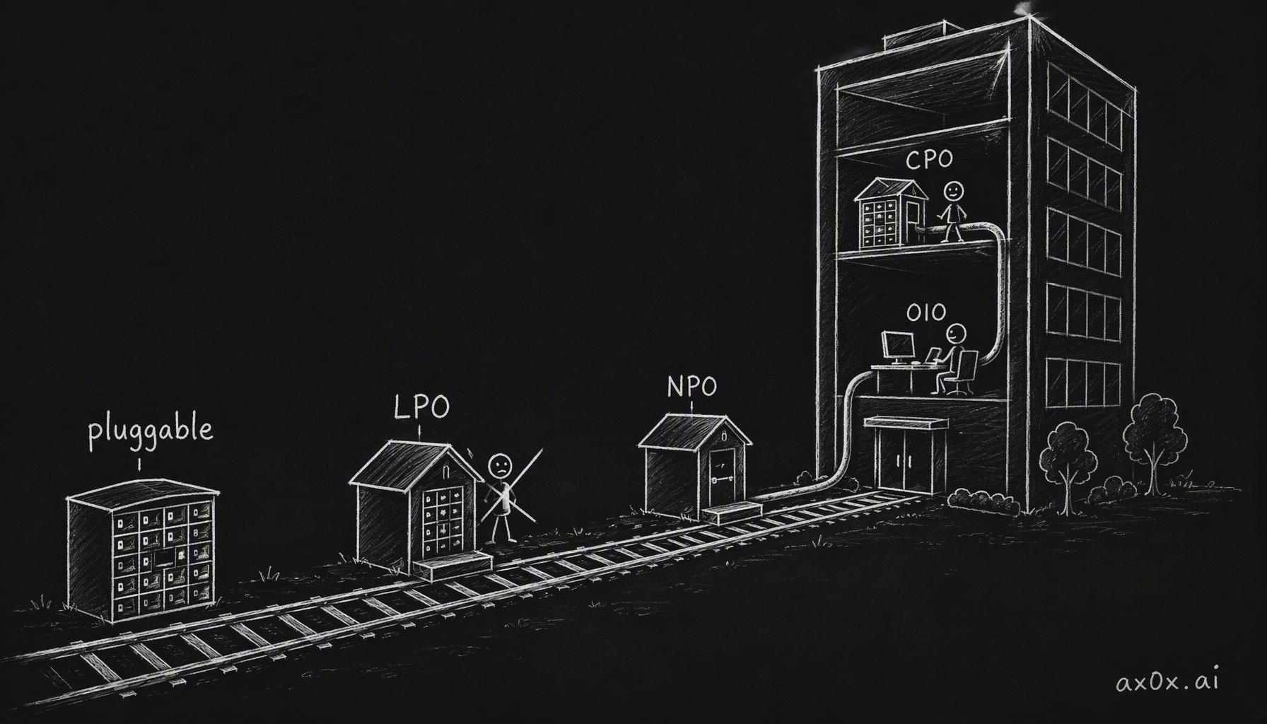 Pluggable, LPO, NPO, CPO, OIO — five packaging schemes, one siting question: how close to the switch chip's office tower do you build the courier depot where light turns back into electricity
Who is pushing CPO
Kevin made a point of one more thing: CPO was not invented by the module makers. Broadcom, NVIDIA and a few big cloud operators are pushing it from the top down, redesigning the whole box. The power saving only shows up when you account at the system level — total box power, packaging density, cost of ownership — and the maintenance and supply-chain costs are also carried by the system side. Broadcom introduced its first-generation CPO chipset in 2021, the second-generation Bailly in 2024, a third generation in 2025, and every step was led by the switch-chip company, with the module vendors supplying optical engines or acting as packaging partners.
敏姐 followed up with a question that sharpened it: could you say the old optical module was a standard product, and the new one is a non-standard, customized part that has to fit the design inside the GPU? Kevin said yes, and the reframing is the useful part. Under pluggables, a module maker could innovate on its own and the customer plugged the result in. With the optical path soldered into the package, the choice of optical components and the repair procedure are decided by whoever makes the switch chip or the GPU. Traditional module vendors have to find a new position. One route goes up, becoming the co-packaging partner that supplies the optical engine — 光迅 working with Huawei and NVIDIA on 3.2T CPO is that path. Another stays with pluggables and LPO. 华工科技 is running NPO and CPO platforms in parallel, a bet on both.
When does CPO mature? Kevin's estimate when the episode was recorded in July was that its flexibility and serviceability are very likely to stay well behind pluggables, so it would take at least two or three years before the first substantial progress shows. Shipping is already happening — Broadcom's Davisson has been going out since last October — but shipping and wide deployment are two different things.
How many of the three roads survive
So who wins in the end? 石磊 asked the question I would have asked: is there path dependence here, where whichever scenario ramps first matures first and the other roads never get their chance? Kevin's answer was that it comes down to how cheap the thing is and how well it works. 敏姐 added that it's an economics question.
In practice the cloud buyer weighs two things: what the module costs to buy, and what the system costs to run over its life — can you swap the part, and can you find the fault when something breaks. Pluggables won't disappear; flexibility, serviceability and multiple vendors bidding against each other are real money in the bill of materials. What CPO wins is the electricity bill at hyperscale. Run the two ledgers in different settings and they come out differently, which is why the three roads will probably coexist for a long while. Kevin's phrasing was that it ends up being whoever's cost comes down first. CPO seeps into the largest, densest deployments a step at a time; the hop between racks stays pluggable territory. Inside the rack it's still copper and LPO — NVIDIA's own next-generation Rubin rack keeps an all-copper scale-up backplane, and SemiAnalysis specifically knocked down the rumor that the Kyber rack was moving to CPO. NVIDIA's CPO today is on the switch side; when GPU-to-GPU scale-up across racks goes optical is not settled yet.
Where do Chinese vendors sit in this? Seven of the world's top ten module makers are Chinese, while the ODSP and the high-end optical chips are still made elsewhere. That's part five.
This series is compiled from episode 75 of the Chinese podcast 十分吸引, "光与电的游戏:有线通讯史的百年之争", with guest Kevin, a chip systems engineer, and hosts 石磊, 敏姐 and 孙悦. The framing is Kevin's; I reorganized it by theme and wrote it up, so any errors are mine. Neither the episode nor this post is investment advice — companies are named only as examples of where the supply chain sits.