How HBM Works — the Memory That Decides Who Wins AI
 How HBM works cover
Pull the lid off an Nvidia B300 module and the logic die — the GPU itself, the thing everyone obsesses over — is not the most expensive part sitting there. The memory is. On a modern AI GPU module, the HBM stacks account for somewhere around 40-50% of the bill of materials. You read that right: the chip that does the math is cheaper than the chips that feed it.
I finance and operate the machines AI runs on. When you actually have to buy these things at scale, you stop thinking of the GPU as "the product" and the memory as "an accessory." The memory is co-equal, often co-dominant, in both cost and availability. And HBM — High-Bandwidth Memory — is the single component that is most sold out, most supply-constrained, and most decisive in who wins the next two years of AI.
This is the centerpiece of the series, so I want to do the one thing most coverage skips: explain how HBM actually works, from the physics up. Because once you see the architecture, every confusing thing about this market — the trillion-dollar market caps, the packaging bottleneck nobody can fix, why China can't just copy it — stops being confusing. It all falls out of one design decision.
Earlier in this series I argued that AI's real bottleneck quietly shifted from compute to bytes — the memory wall — and walked through how ordinary DRAM works, one transistor and one leaky capacitor per bit. HBM is what you get when you take that DRAM and refuse to accept its layout.
HBM is DRAM rotated 90 degrees
Here's the whole idea in one sentence: ordinary DRAM lives flat, spread across a circuit board and talked to through a narrow channel; HBM takes the same DRAM dies, stacks them vertically into a tower, drills thousands of wires straight down through the silicon, and parks that tower a few millimeters from the GPU.
That's it. That's the trick. Everything else is consequence.
Think about why this matters. A standard DDR5 memory channel is 64 bits wide. To move data, you run that channel at a high clock and ship 64 bits at a time down a long copper trace to a DRAM module sitting an inch or two away. You can add channels, but each one costs you pins, board area, trace routing, and power. Distance is the enemy — the farther the signal travels, the more energy it burns and the harder it is to run fast and clean.
HBM throws out the long copper trace. Each HBM stack talks to the GPU over a 1024-bit-wide interface. That is sixteen DDR5 channels' worth of width, in a single stack, running over a connection that's millimeters long instead of inches. You don't need a screaming clock speed to move a firehose of data — you just make the pipe absurdly wide and keep it short. Wide and close beats narrow and fast, and it beats it on power too, which matters enormously when you're packing a hundred kilowatts into a rack.
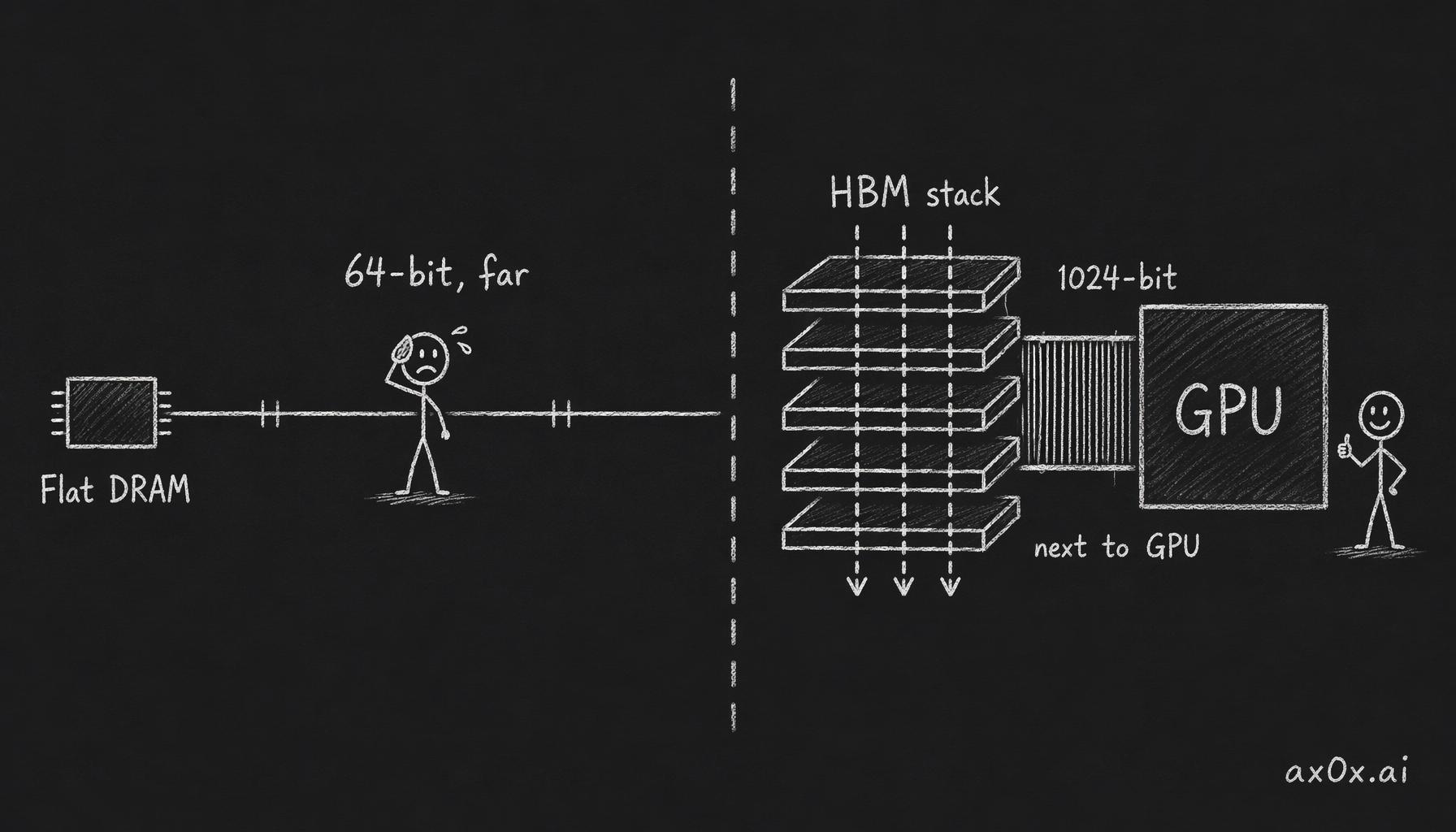 Where HBM's bandwidth comes from: stack the DRAM vertically, drill TSVs down through it, widen the bus to 1024 bits and park it millimeters from the GPU — wide and close beats narrow and far
So HBM is not "DRAM but faster." The cells are the same leaky capacitors I described in the DRAM piece. What changed is the delivery — the geometry of how bits get from the cell to the processor. HBM trades a ferociously difficult manufacturing process for a data path so wide that bandwidth stops being the thing you ration.
And notice what the wide-and-short bet buys you on the power side, because in a data center power is the real currency. Moving a bit costs energy, and most of that energy goes into driving the signal across distance at speed. If you can get your bandwidth from width instead of frequency, and your distance from millimeters instead of inches, you get the same firehose for a fraction of the picojoules-per-bit. HBM delivers far more bandwidth per watt than any flat memory could. When you're trying to keep a rack of accelerators fed without melting the building, that efficiency isn't a nice-to-have — it's the only reason the architecture is viable at all.
A stack is a controller with DRAM bolted on top
Let me build one up, bottom to top.
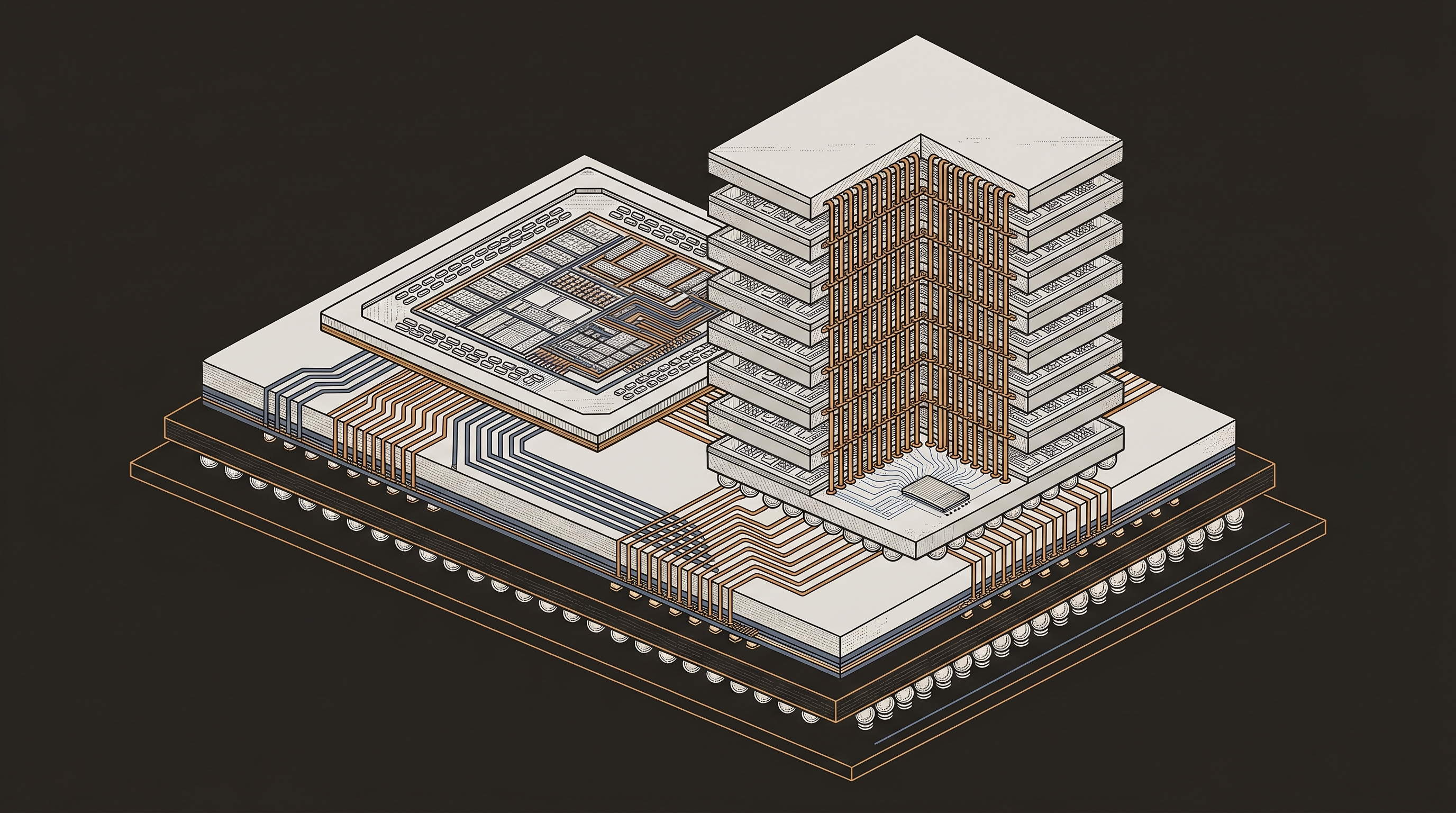
At the bottom is a base logic die. It's the brains of the stack — the memory controller, the I/O, the test and repair logic. It's the part that talks to the GPU.
On top of the base die you stack the actual DRAM dies — the memory itself. Today's volume product, HBM3E, stacks 8 or 12 of them; the leading edge is pushing to 16-high. The industry shorthand is "8-Hi," "12-Hi," "16-Hi." More dies means more capacity per stack, and also more ways for the whole thing to go wrong, which we'll get to.
Running vertically through the entire tower — through every die — are through-silicon vias, or TSVs. These are the vertical wires. A modern stack has thousands of them, each one a microscopic copper-filled hole etched straight down through the silicon, carrying signal and power from the base die all the way to the top. TSVs are what make the stack a single electrical object instead of a pile of separate chips. They are also the single hardest thing about building HBM.
The finished stack — base die plus DRAM dies, bonded together, threaded with TSVs — then sits on a silicon interposer: a thin slab of silicon, etched with ultra-fine wiring, that the GPU also sits on. The interposer is what lets the 1024-bit-wide connection between GPU and HBM exist at all. You cannot route a thousand-plus wires across a normal printed circuit board at these densities. You need silicon-grade wiring, on a silicon substrate, with the GPU and the memory sitting on the same slab. That slab, and the process of building on it, is CoWoS — and it deserves its own section, because it's a bottleneck the entire industry is hostage to.
A flagship GPU doesn't carry one stack. A B300 carries eight of them ringed around the logic die, all on one interposer. Eight stacks × 1024 bits each is an 8192-bit-wide path between the processor and its memory. That's the firehose.
It's worth pausing on what the base logic die does, because it's where HBM stops being a passive memory part and starts being something smarter. The base die doesn't just pass signals through; it manages the stack — addressing the right die and the right cell, handling the test-and-repair logic that lets the stack route around defective bits, and presenting a clean interface to the GPU so the processor doesn't have to know it's talking to a 12-story tower. In a flat DDR5 system, that controller intelligence lives on the GPU or CPU side. HBM pulls a chunk of it down into the bottom of the stack. Remember that detail — it's the seam that HBM4 pries open, and it's where the competitive map gets redrawn.
Each generation just makes the pipe wider
Each generation of HBM has widened or sped up the firehose. The numbers, per stack:
| Generation | Bandwidth per stack | Capacity per stack | Status |
|---|---|---|---|
| HBM2 | ~256 GB/s | up to 8 GB | early |
| HBM2E | ~460 GB/s | up to 16 GB | superseded |
| HBM3 | ~819 GB/s | 16-24 GB | superseded |
| HBM3E | ~1.2 TB/s | 24-36 GB | current volume |
| HBM4 | ~2+ TB/s (up to ~3.3 on early 12-Hi) | 36-64 GB | 2026+, projected |
(Bandwidth figures are per-stack peak, directional, per JEDEC and industry roadmaps.)
Two things are worth sitting with. First, the jump from HBM2's ~256 GB/s to HBM3E's ~1.2 TB/s is roughly 5x in a few years — bandwidth scaling that ordinary DDR memory comes nowhere near. Second, HBM4 doubles the interface width again, from 1024 bits to 2048 bits per stack. That's the headline change for the next generation, and it's not a clock-speed trick — it's literally a wider pipe, which is the whole HBM philosophy taken one step further.
Now multiply by stack count on the GPU. The cleanest way to see the trend is in HBM content per flagship GPU: 80 GB on the H100 (2022), 141 GB on the H200 (2024), ~192 GB on the B200, ~288 GB on the B300 (2025). The honest framing — and I'm careful here because the marketing tends to overclaim — is that HBM content per flagship GPU has roughly doubled about every two years: 80 GB in 2022 to 288 GB in 2025. That growth is why memory keeps eating a bigger share of the module cost, and why memory demand is growing faster than GPU unit shipments. Every new GPU doesn't just need an HBM stack — it needs more HBM than the last one.
This is the demand curve that breaks intuitions. If you assume memory demand tracks GPU shipments one-for-one, you'll under-forecast badly. Each generation needs more HBM per unit and more units are shipping. The two multiply. That compounding is a big part of why the memory wall became an economic event and not just a technical one — the appetite for bandwidth and capacity is growing faster than any flat extrapolation of GPU counts would suggest, and the supply chain that makes HBM can't flex to meet it on the same timeline.
Why HBM is hostage to CoWoS
Here's the thing people miss: you cannot buy HBM and a GPU and bolt them together yourself. The whole assembly — GPU logic die plus the HBM stacks plus the silicon interposer they all sit on — has to be manufactured as one advanced-packaging operation. At TSMC, that process is called CoWoS — Chip-on-Wafer-on-Substrate.
CoWoS is where the GPU die and the HBM towers get placed onto the silicon interposer with micron-level precision and bonded into a single package. No CoWoS, no AI GPU. It doesn't matter how many HBM stacks SK Hynix can make or how many logic dies TSMC can fab — if you can't package them together, you have parts, not products.
And CoWoS is its own bottleneck, arguably the single tightest chokepoint in the entire AI hardware supply chain. TSMC has been roughly doubling CoWoS capacity every year — and it is still constrained, with demand running ahead of supply (per TSMC's own commentary and SemiAnalysis tracking). When you hear that GPU shipments are gated, the gate is very often here: not in the logic fab, not in the memory fab, but in the packaging step that marries the two. I wrote about this dynamic in TPU vs GPU — everyone, Nvidia and Google alike, is fighting over the same scarce CoWoS and HBM capacity. The chip design stopped being the moat a while ago. The packaging is the moat now.
There's a deeper reason CoWoS can't just be ramped overnight, and it's worth understanding because it's the same reason HBM can't. The interposer is itself a piece of silicon, processed on wafer-scale tooling, with its own yield curve. Every defect on a large interposer can scrap a finished assembly that already has an expensive GPU and several thousand dollars of HBM bonded to it. So the cost of a CoWoS yield miss isn't the interposer — it's everything sitting on top of it. That's why you can't fix the bottleneck by throwing cheap capacity at it. The capacity has to be good capacity, and good capacity at this complexity is exactly the thing that takes years and a TSMC-grade process to build.
This is the part that should reframe how you read every "GPU shortage" headline. The shortage is rarely the GPU. It's the memory next to it and the packaging that holds them together. When I'm sizing how fast a cluster can actually come online, the GPU order is almost never the long pole. The long pole is somewhere in this packaging-and-memory chain, and no amount of GPU allocation fixes it.
HBM4 quietly changes who wins
For most of HBM's life, the base logic die at the bottom of the stack was a simple thing, fabbed by the DRAM maker itself on a trailing process. It was a commodity floor for a commodity tower.
HBM4 breaks that. With HBM4, the base logic die becomes a customer-specific logic die that can be fabricated by a foundry — read: TSMC — on an advanced process. The memory maker stacks the DRAM; the foundry builds the brains. The base die can now carry custom logic tuned to a specific customer's GPU.
That sounds like a footnote. It's actually a strategic earthquake. It turns HBM from a commodity memory part into a semi-custom logic-plus-memory product — and it reshuffles who captures the value.
Look at the alignment it creates. SK Hynix, the HBM leader, has partnered with TSMC for HBM4 base dies — so the memory champion and the packaging-and-logic champion are now joined at the hip. Samsung, which owns its own foundry, can build the whole thing in-house — a vertical-integration bet that the rest can't match. Suddenly HBM isn't a part you order off a spec sheet. It's a co-design relationship between a memory maker, a foundry, and the GPU vendor. The companies that own more of that triangle capture more of the margin. This is the same lesson from compute generally: the more of the stack you control, the more of the value you keep.
Why the moat is yield, not secrets
So who actually makes this stuff? Three companies, and the gaps between them are real.
SK Hynix leads, with somewhere north of 50% of the HBM market (per TrendForce). It was first to ship HBM3 and first to HBM3E, and it's the primary HBM supplier to Nvidia. When people say HBM is sold out, they mostly mean SK Hynix's HBM is sold out. And "primary supplier to Nvidia" is not a small phrase — it means the company that makes the most-wanted accelerator on Earth depends, for its scarcest component, on one memory maker being good at the hardest part of the process. That dependency is a large part of why HBM pricing has been firm even as commodity DRAM swings around: the buyer has nowhere else to go in volume, at least not yet.
Samsung is the integrated giant — it makes both logic and memory — and has been working to catch up on HBM3E qualification while playing its in-house-foundry card for HBM4.
Micron, the lone US maker, is ramping 12-Hi HBM3E and gaining share, and it carries the additional tailwind of the US reshoring narrative.
Now — why only three? Why can't a well-funded newcomer, or China, just copy the design and flood the market? The HBM spec is published by JEDEC. The architecture isn't secret. The moat isn't the idea. The moat is yield.
Walk back through the anatomy and count the ways it can fail. You're etching thousands of TSVs straight through silicon — each one has to be void-free and aligned across every die in the stack. You're bonding 12 or 16 wafer-thin dies into a tower where a single bad die can scrap the whole stack, so you need known-good-die testing before you ever bond. You're dissipating heat from the middle of a vertical sandwich, where the inner dies have nowhere for their heat to go. And you're fighting warpage — stacks of thin silicon want to bow, and a bowed stack won't bond or sit flat on the interposer. Thousands of vertical vias, sixteen stacked dies, thermal stress, mechanical warpage — every one of those is a yield killer, and they compound.
And the killer detail is how those failure modes interact. Each die you add to the stack lowers the odds the whole tower comes out good, because the stack only ships if every die in it is good and every TSV connection holds. Yield on a 12-Hi stack is structurally harder than on an 8-Hi stack, and 16-Hi harder still — the math compounds against you with every layer. That's why moving up the stack-height ladder isn't a free capacity gain; it's a fresh yield fight each time. The companies that win the next generation are the ones who solve that fight first, not the ones who announce the spec first.
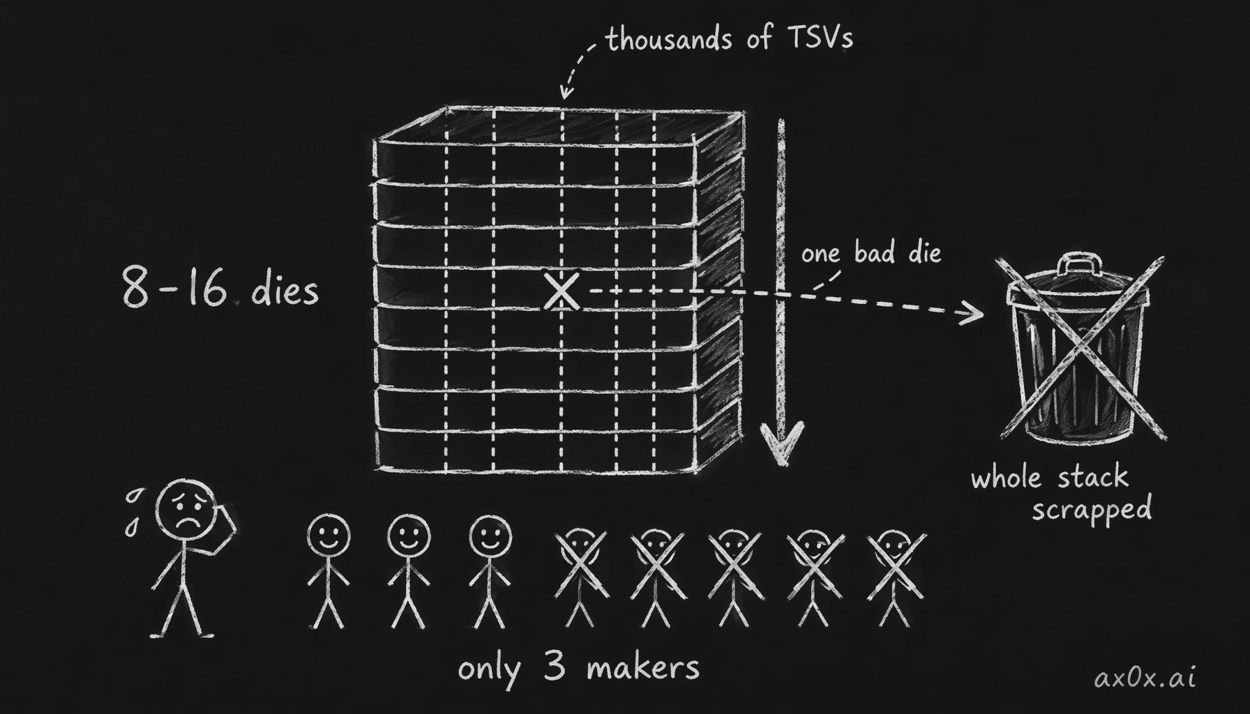 HBM's moat is yield: drill thousands of TSVs through a stack of 8-16 dies, and one bad die or one bad via scraps the whole tower — failure compounds with every layer, which is why only three makers survive
That's why this is a three-horse race. Anyone can read the spec. Almost no one can build it at acceptable yield, at volume, generation after generation. The difficulty is the moat — the same way it is for TSMC at the leading edge. China's CXMT is reportedly sampling HBM (to Huawei, among others), but volume is realistically a 2027-28 story. Catching up on a yield curve this steep takes years, not a fab order — and by the time you've matched today's product, the leaders have moved a generation ahead.
The difficulty is why three companies crossed a trillion dollars
Here's where it all lands. In May 2026, all three memory makers — Samsung, Micron, and SK Hynix — crossed a $1 trillion market cap: Micron and SK Hynix within a day of each other in late May, Samsung a few weeks earlier. SK Hynix's stock is up roughly tenfold over the trailing year. These are companies that, for most of their history, were the textbook example of a brutal, low-margin, boom-bust commodity business. Memory was the business nobody wanted to be in.
That repricing is not a story about demand alone. Demand explains why memory got scarce. It doesn't explain why only three companies get to satisfy it. The architecture I just walked through — DRAM rotated 90 degrees, threaded with thousands of vias, packaged by a process only TSMC has scaled — is what turns "scarce" into "scarce and unclonable." A commodity with a moat is no longer a commodity. That's the whole repricing in one line.
I'll close on the part that gets under my skin as someone who buys this hardware. We spent two years calling this the compute era and pointing at Nvidia. But the thing that's actually sold out, the thing that's actually repricing companies into the trillions, the thing that actually gates how fast you can stand up an AI cluster — is the memory stacked beside the logic, and the few-millimeter slab of silicon holding them together. The hardest part of an AI GPU was never the part that does the math.
In the next piece I'll follow the money: the memory supercycle — what happens to the whole market when the cheapest input becomes the scarcest one, and whether this cycle, like every memory cycle before it, eventually breaks.
Related reading
- The Memory Wall — why AI's bottleneck shifted from compute to bytes
- How DRAM Works — the leaky capacitor that HBM stacks vertically
- The Memory Supercycle — the trillion-dollar repricing of memory
- Beyond the Memory Wall — HBF, CXL, and what comes after HBM
- TPU vs GPU — why the CoWoS and HBM bottleneck shapes the whole compute market
- Compute Is the Root of the AI Economy — owning more of the stack captures more of the value


