How NAND Flash Works — From Your SSD to the AI Data Center
 How NAND flash works, from your SSD to the AI data center
There is one chip behind your USB stick, your phone's storage, your laptop's SSD, and the petabyte-scale drives stacked inside AI data centers. It is the same fundamental technology in all of them, scaled up and down. That chip is NAND flash, and it is the reason a terabyte of storage costs you a coffee instead of a paycheck.
I finance GPU infrastructure for a living — I buy the clusters and build the data centers, which means I spend a lot of time staring at the bill of materials for a modern AI server. For years NAND was the line item I thought about least. It was the cheap, slow, reliable bucket at the bottom of the stack where data went to sit. The expensive, interesting, scarce stuff was up top — the logic die, and the HBM bolted next to it. NAND was an afterthought.
That's changing fast, and what makes it interesting is that NAND isn't changing at all. The same property that made it cheap and boring for forty years is the property AI suddenly wants. To see why, you have to understand how the thing actually works — and the good news is that the physics is simpler than DRAM's, and the economics fall straight out of the physics.
This is Part 3 of The Memory Stack. Part 2 covered DRAM — the fast, forgetful working memory that loses everything the instant you cut power. NAND is its opposite in almost every way.
The whole physics fits in one sentence
NAND is non-volatile: it remembers without power. A USB stick sitting in a drawer for a year still has your files. DRAM in the same drawer would be blank within a fraction of a second.
Here's the trick. Each storage cell is a tiny transistor with an extra, electrically isolated layer in the middle — historically a "floating gate," in modern 3D NAND a "charge-trap" layer. To write a bit, you shove electrons across an insulating barrier and strand them on that island. Because the island is insulated on all sides, the electrons have nowhere to go. They just sit there, for years, with the power off. The amount of charge trapped is what the cell "remembers."
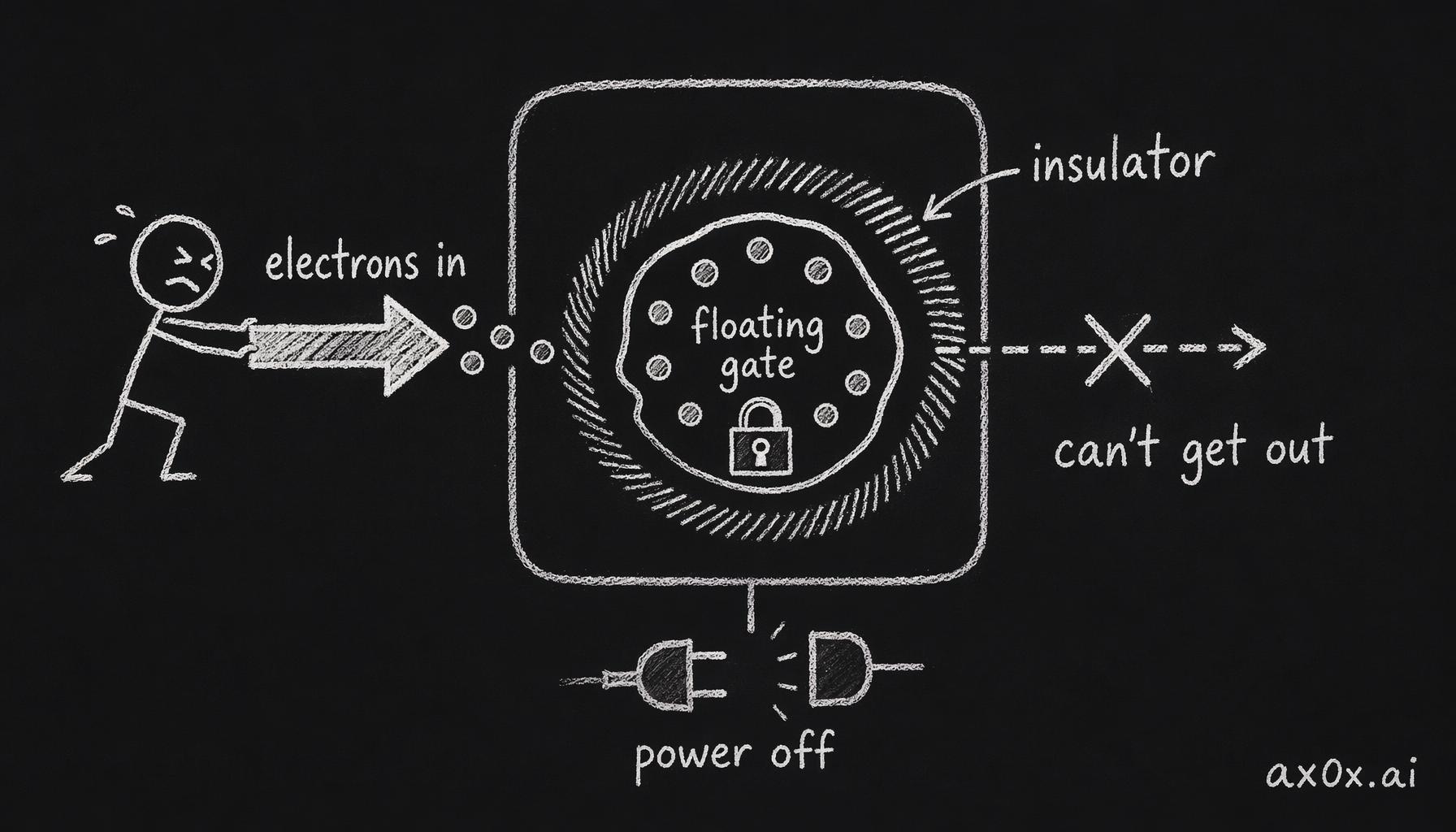 NAND stores a bit by physically trapping electrons on an insulated island — they go in, can't get out, and stay put even with the power off
That's the entire idea. Permanence comes from physically trapping electrons behind an insulator. And — this is the part that matters for everything downstream — the only way to write or erase is to forcibly drag those electrons through that insulator using high voltage (a quantum-tunneling effect with the unfriendly name Fowler-Nordheim tunneling). Every single time you do it, the barrier takes a little damage. A few traps form in the insulator; over many cycles they accumulate, the barrier gets leaky, and eventually the island can no longer reliably hold its charge. Flash doesn't wear out from sitting still — a chip can hold data for years untouched. It wears out from being written.
Reading, by contrast, is gentle and indirect. You don't pull the electrons back out to check them. You apply a voltage to the cell and measure whether it conducts, which tells you how much charge is sitting on the island without disturbing it. That asymmetry — cheap, harmless reads versus expensive, damaging writes — turns out to be the entire reason AI and NAND are about to become friends. But I'm getting ahead of myself.
That's the central fact of NAND. Hold onto it, because the entire economics of the technology fall out of it.
The tradeoff that runs the whole business
Once you can trap charge on an island, an obvious question follows: why store just one bit per cell? If you can detect how much charge is on the island — not just present-or-absent, but four levels, eight levels, sixteen — then a single physical cell can hold two, three, or four bits at once. Same silicon, more data, lower cost per gigabyte.
This is the lever the entire NAND industry has been pulling for two decades, and it has a name for each setting:
| Type | Bits/cell | Voltage levels | Rough endurance (P/E cycles) | Role |
|---|---|---|---|---|
| SLC | 1 | 2 | ~50,000–100,000 | Industrial, caches, where reliability is everything |
| MLC | 2 | 4 | ~3,000–10,000 | Older premium consumer / enterprise |
| TLC | 3 | 8 | ~1,000–3,000 | The mainstream — most SSDs and phones today |
| QLC | 4 | 16 | ~100–1,000 | High-capacity, read-heavy, cheapest per GB |
| PLC | 5 | 32 | experimental | Lab / roadmap, not a shipping product |
(P/E = program/erase cycles, the number of times a block can be written and wiped before it stops holding charge reliably.)
Read that endurance column top to bottom. SLC survives on the order of a hundred thousand writes. QLC might survive a few hundred. That's not a small difference — it's two to three orders of magnitude, and it's not a manufacturing flaw. It's geometry.
When you cram four bits into one cell, you're carving the same physical charge range into sixteen distinguishable levels instead of two. The voltage windows that separate "this value" from "that value" get razor-thin. A tiny amount of charge leaking off the island — or a tiny amount of damage to the insulator from the last few thousand writes — and the cell drifts across a boundary and reads back the wrong number. SLC, with two levels and a yawning gap between them, can be wrong by a lot and still resolve to the right bit. QLC has sixteen levels packed into the same range; it has almost no margin for error at all.
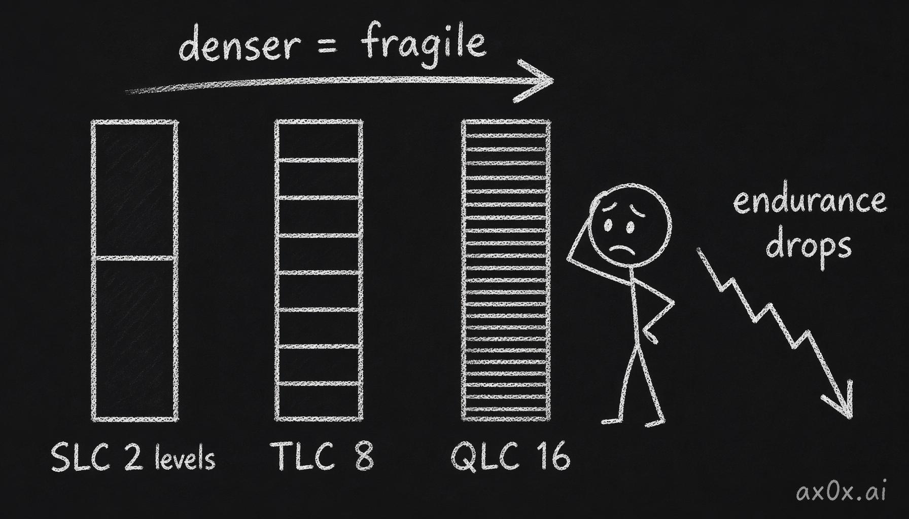 Cramming more bits into a cell slices the same voltage range into more, thinner levels — so higher density buys you far lower endurance
That cascades into everything. Denser cells are slower to write, because you can't just blast charge in — you have to nudge it in carefully and verify, step by step, to land on exactly the right one of sixteen levels. They're slower to read, because sensing a fine level takes more time than sensing present-versus-absent. They tolerate fewer writes before the windows blur past recovery. And they lean hard on error-correcting codes — modern QLC would be unusable without aggressive ECC quietly fixing bits behind the scenes on every read.
That's the deal, and there's no free lunch in it: every bit of density you buy, you pay for in endurance. Denser and cheaper, but slower and more fragile. This is why a 4TB consumer SSD is affordable and why it's also the kind of drive you'd never use as a write-heavy database log. It's why NAND has always been "cold storage" — the place data goes to rest, not the place it gets churned. Hold that thought.
Scaling stopped meaning "smaller" and started meaning "taller"
For most of chip history, getting cheaper meant getting smaller: shrink the feature, pack more cells per square millimeter, repeat every couple of years. NAND rode that curve down to the mid-teens of nanometers in the mid-2010s — and then hit a wall. Below that, cells sit so close together that the charge on one island starts to disturb its neighbors. Squeeze further and the bits literally corrupt each other. Planar (2D) NAND had run out of room.
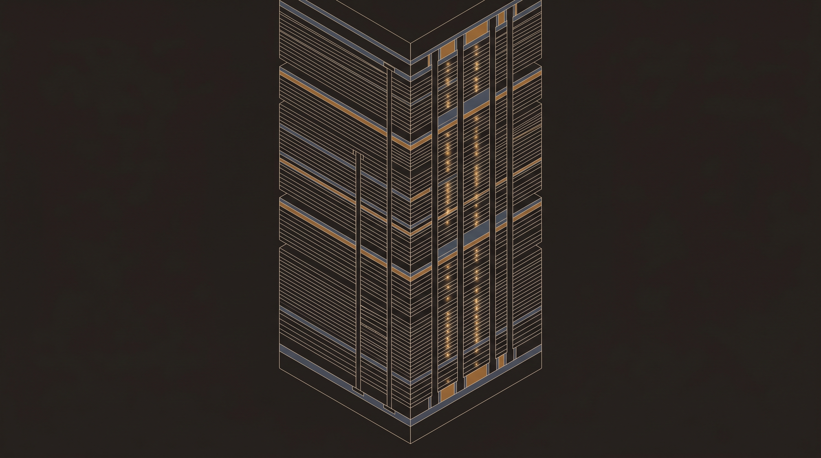
The fix was one of the great pivots in semiconductor history: stop shrinking, start stacking. Instead of packing cells tighter on a flat plane, build them up — layer on layer on layer, a high-rise of memory cells stacked vertically on the same footprint. This is 3D NAND, and it reset the entire scaling story.
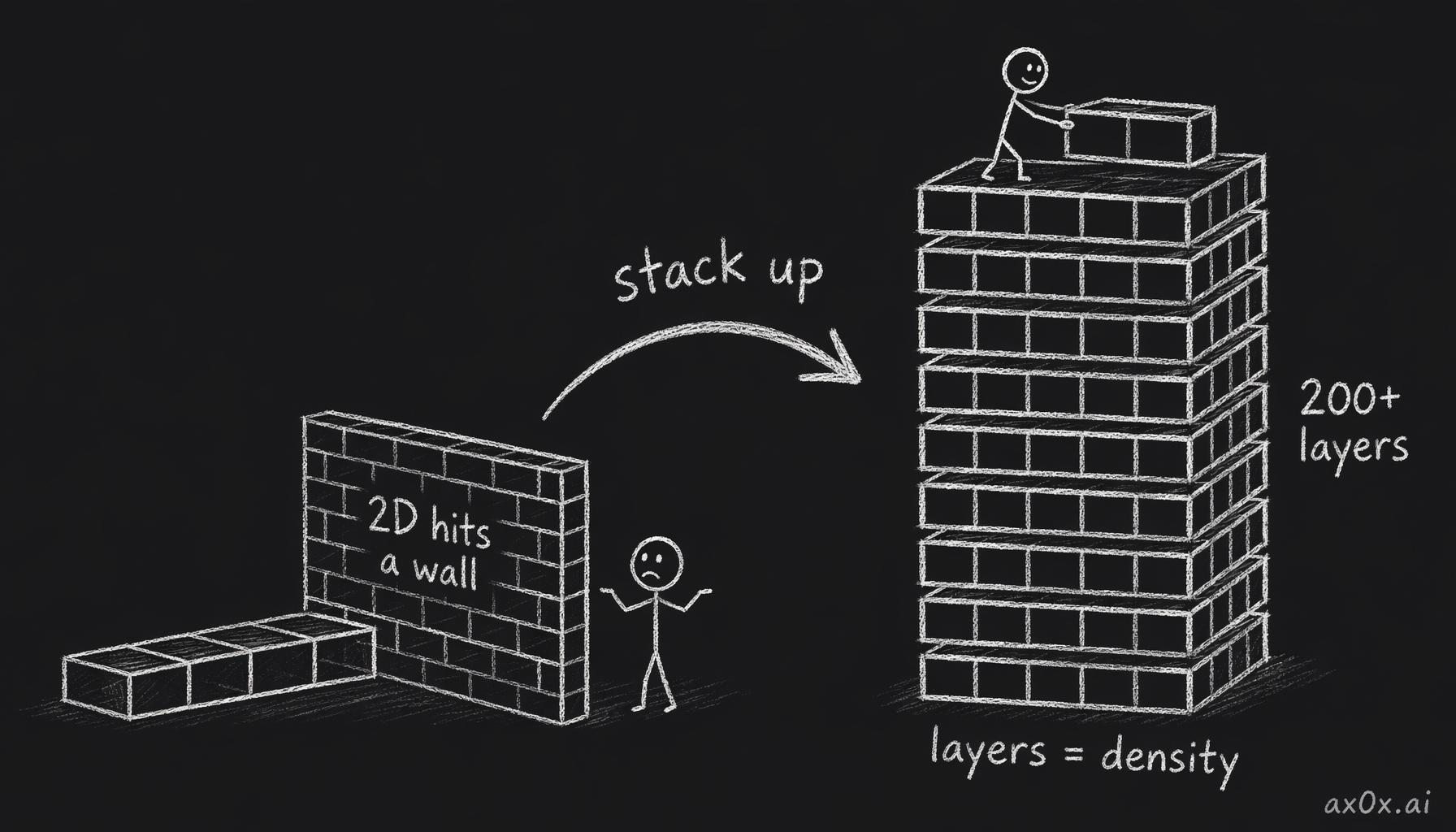 Once flat shrinking hit a physical wall, NAND stopped shrinking cells and started stacking them vertically like a high-rise, gaining density from layer count
The layer count is the new Moore's Law of storage. The first commercial 3D NAND around 2013 stacked 24 layers. The leading parts now shipping in volume are at roughly 280 to 321 layers — Micron's 276-layer G9, Samsung's 286-layer V9, SK Hynix's 321-layer part. The public roadmaps point toward 400, 500, and eventually 1,000 layers by around 2030.
It's worth pausing on how hard this is, because the engineering is genuinely absurd. Stacking 300 layers means drilling holes straight down through all 300 of them and lining every hole with the same materials, perfectly, with no defect anywhere along a vertical channel taller than it is wide by a ratio that keeps climbing. A single flaw kills the whole string. The leading makers have started building chips in two stacks bonded together ("string stacking") precisely because etching one clean 300-deep hole is at the edge of what's physically possible. This is not a coasting industry; it is sprinting up a wall.
But it's why storage keeps getting cheaper even though the old shrink-the-feature playbook stalled a decade ago. The cost-per-bit curve didn't break; it just changed axes. The industry stopped fighting physics in the horizontal plane and started winning in the vertical one. Every new layer is more capacity on the same wafer, which is more terabytes for the same dollar. Stacking and bit-cramming compound: a 300-layer QLC die holds vastly more than a 24-layer SLC one on the same patch of silicon — which is the whole reason a terabyte costs what a sandwich costs.
Two footnotes that explain the rest of it
NOR vs NAND. You'll see "NOR flash" mentioned and wonder why it doesn't show up in your SSD. They're cousins with opposite jobs. NOR flash is random-access and supports execute-in-place — a processor can run code directly out of it, byte by byte. It's fast to read, expensive, and small, so it lives in the boot ROM and firmware of embedded devices. NAND is organized into pages and blocks, not individual bytes; you can't read one byte at a time, but you get vastly higher density and far lower cost. That's the whole reason NAND, not NOR, won mass storage. NOR runs the code; NAND holds the data.
Pages, blocks, and the erase problem. NAND has one deeply annoying quirk that shapes everything built on top of it: you write in small units (pages, a few kilobytes) but you can only erase in large units (blocks, made of hundreds of pages). You cannot overwrite a single page in place. To change one byte, the drive has to read the whole block, modify it, write it somewhere fresh, and erase the old block later. That mismatch — fine-grained writes, coarse-grained erases — is the original sin that all SSD complexity flows from.
That erase problem spawns two more terms worth knowing. Wear-leveling: remember that every write damages a cell, and that QLC might only take a few hundred writes? If your operating system kept rewriting the same physical block, that block would die in days. So every SSD runs a controller (the flash translation layer) that spreads writes evenly across all the cells, so no single block gets hammered. And write amplification: because of that page-versus-block mismatch, one logical write from your computer can trigger several physical writes underneath as the controller shuffles live data around to free up a block to erase. A write-amplification factor of 3 means every gigabyte your OS writes becomes three gigabytes of actual flash wear. That hidden multiplier is why enterprise SSDs are rated in "drive writes per day" and why the endurance numbers in that table above matter so much in practice. The smartest part of a modern SSD isn't the flash — it's the controller keeping the fragile flash alive.
The twist: AI is dragging NAND onto the hot path
For decades the job description was settled. DRAM is the hot, fast, expensive working memory. NAND is the cold, cheap, durable archive. The two never really competed — they did different jobs at different temperatures.
AI is breaking that clean split.
The reason is the memory wall — the gap between how fast compute got and how slowly memory bandwidth and capacity kept up. The most expensive, most scarce memory in an AI server is HBM, the stacked DRAM bolted to the GPU. There is never enough of it. And when you run inference at scale, a huge amount of HBM gets consumed by the KV cache — the model's running memory of the conversation so far. Some of that cache is hot (being used this instant); a lot of it is cold (a long context the model might need again later, but not right now).
Holding cold KV-cache in scarce, expensive HBM is like parking a car you won't drive until next week in the most expensive garage in the city. The economics are offensive once you see them. HBM is the single priciest, most supply-constrained component in the whole server — when I underwrite a cluster, it's a meaningful slice of the bill — and a chunk of it sits there holding context the model isn't using this second. NAND is orders of magnitude cheaper per gigabyte. The arbitrage writes itself.
So the industry started doing the obvious thing: spill the cold parts down the hierarchy onto cheap, dense NAND, and pull them back up only when needed. NVIDIA's CMX — Context Memory eXtension, a BlueField-4 DPU-managed NVMe tier (it debuted as ICMS at CES 2026 and surfaced as CMX around GTC 2026) — does exactly this: it extends HBM by spilling cold KV-cache out to NAND. It doesn't replace HBM; it gives HBM somewhere cheap to offload to. The hierarchy I described in Part 1 — SRAM, DRAM, NAND, getting bigger and slower as you go down — isn't just a static picture anymore. AI is actively shoveling data up and down it in real time, and NAND just got promoted from "the bottom shelf" to "the overflow tank for the most expensive memory in the building."
You can feel the pull in the order books. Through 2025 and into 2026, AI demand drove a surge in enterprise QLC SSDs — the densest, cheapest, most write-fragile flash there is. And notice why QLC, of all things, is the one winning here. Go back to that asymmetry: reads are gentle, writes are what kill flash. AI inference is overwhelmingly read-heavy — you load a model, you stream a cache, you read it back many times and rarely rewrite it. That's the one workload profile that doesn't punish QLC's pathetic endurance, while it desperately wants exactly QLC's strength: the most capacity per dollar of any memory you can buy. The weakest, cheapest flash on the table turns out to be the perfect match for the most demanding workload of the decade. The cold-storage tier is suddenly strategic.
And the boldest version of this is to stop treating NAND as merely a spillover tier at all. SanDisk's High Bandwidth Flash (HBF) proposes stacking flash with TSVs — through-silicon vias, the same vertical wiring trick HBM uses to stack DRAM — and putting it right next to the GPU where HBM lives. The pitch: something like 8 to 16 times the capacity of HBM at comparable total system cost — i.e. far better cost per gigabyte (SanDisk's framing is similar overall cost, not cheaper), in pre-production with samples expected around the second half of 2026. If that works, NAND wouldn't just be the overflow tank anymore — it would be sitting in the same premium real estate as HBM itself, which is a remarkable destiny for the chip everyone treated as the cheap bucket at the bottom. I'll get into HBF, CXL, and the rest of the workarounds in Part 6 — they're the toolkit the industry is assembling to climb the memory wall.
None of this means NAND becomes DRAM. It can't — the physics that make it cheap also make it slow and fragile, and no amount of stacking changes that. What's happening is subtler and more interesting: the system is learning to use NAND's specific shape on purpose, building tiers and controllers and offload paths that route the read-heavy, capacity-hungry, write-light parts of the AI workload exactly to the memory that's good at being read-heavy, capacity-hungry, and write-shy. The technology didn't transform. The job description around it did.
Here's the through-line. NAND got cheap by trading endurance for density — and for forty years that fragility is exactly what kept it cold, kept it cheap, kept it at the bottom of the stack. The same property is now its opening: AI inference is read-heavy and capacity-starved, which happens to be the one workload that doesn't care about NAND's weakness and craves precisely its strength. The chip that got cheap by being fragile is being promoted because the new boss doesn't mind the scars.


