Beyond the Memory Wall: The Workarounds, the Challengers, and the Turn
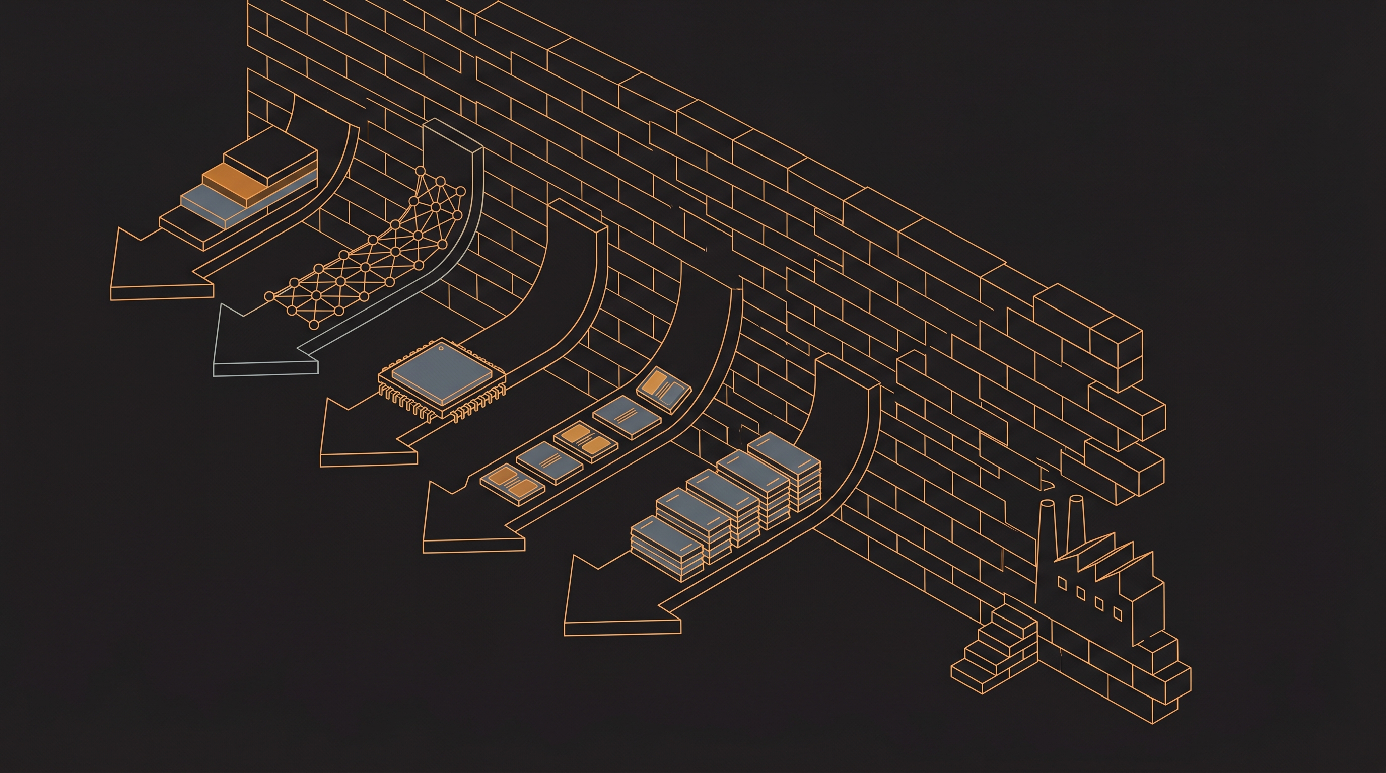 Diagrams of memory tiering, wafer-scale chips, and flash-stacked-like-HBM, with a Chinese fab climbing a wall
I finance the machines AI runs on. Five posts ago I said the surprise of that job was that the scarcest, priciest thing inside a modern AI server isn't the logic die — it's the memory stacked next to it. Everything since has been an attempt to take that one sentence apart honestly: how DRAM works and why it got scarce, how NAND trades endurance for density, why HBM is the part that decides who wins, and why this cycle's valuations might — might — be different.
This is the last one. It's the "what now" post. Because if a single component becomes half the cost of the most important chip in the world, you don't just sit there and pay. Every smart team in the industry is, right now, attacking that wall from a different angle. None of them breaks it in 2026. But the shape of how they fail to break it tells you something the earnings calls won't: where the turn in this cycle is, and isn't, going to come from.
A wall this expensive gets attacked from every side at once
The thing to hold in your head is that "the memory wall" isn't one problem. It's a bundle: bandwidth (the firehose into the compute die), capacity (how much you can hold close), and cost (HBM is roughly half the bill of materials of an AI GPU). Each workaround attacks a different face of it. Ranking them by how radical the bet is:
The pattern that emerges is the whole point of this piece, so I'll say it up front and then earn it: almost every one of these routes around the wall instead of through it, and almost every one of them ends up making NAND a hotter, more active layer than it has ever been. The cold-storage chip from post 3 is being dragged into the inference loop from four directions at once.
NVIDIA's move is the least radical and the most telling
Start with NVIDIA, because what they did is the most boring of the five and therefore the most informative.
The thing surfaced as ICMS at CES in January 2026 and got the cleaner name CMX — Context Memory eXtension — around GTC in March. The pitch deck framing is "AI-native storage." The honest engineering description is narrower and more interesting: it's a tiering layer, run by a BlueField-4 DPU, that spills cold KV-cache out of HBM down to an NVMe flash tier and pulls it back when a request needs it.
To see why that matters you have to know what KV-cache is. When a model generates a long response, every token it produces gets cached so it doesn't recompute the whole context each step. On long contexts that cache can balloon to dozens of gigabytes per request — and it sits in HBM, the single most expensive memory in the machine, often doing nothing while it waits to be reused. You are renting Manhattan square footage to store furniture you might need next week.
CMX's bet is: don't. Keep the hot, active KV in HBM; let the dormant KV fall down to a NAND tier the DPU manages; prefetch it back ahead of decode. NVIDIA quotes 5x tokens per second and 5x better power efficiency versus traditional storage; VAST Data showed time-to-first-token dropping from 65 seconds to 3 when a long context is fetched from the tier instead of recomputed on the GPU.
Here's the part the headlines got wrong, and it's the load-bearing correction of this whole section: CMX does not replace HBM, and it is not a generic "prefetch NAND to dodge HBM" trick. It extends HBM. It stops dormant data from monopolizing the expensive layer so the expensive layer can do more work. NVIDIA — the company that sells you the HBM — is not trying to sell you less of it. They're trying to make each gigabyte of it carry a bigger workload, and they're doing it by promoting NAND from warehouse to active participant. That's the tell. The most powerful company in the stack looked at the wall and decided the play was to use HBM better, not to abandon it.
CXL pools memory beautifully on a slide and awkwardly in production
The next angle out is pooling. The idea is genuinely elegant: instead of stranding DRAM inside each server (where it's either underused or short), put it in a shared pool over the PCIe-based CXL fabric and let any host draw from it on demand. Microsoft Azure put the first production CXL VMs into the field in November 2025. CXL 4.0 landed the same month — 128 GT/s on PCIe 7.0, bundled ports pushing toward 1.5 TB/s. On paper, the capacity problem dissolves: terabyte-scale DRAM pools, allocated like cloud storage.
In practice there's a tax, and it's latency. Local DRAM answers in ~80 ns; CXL-attached memory lands around 140–200 ns. That's fine for cold or capacity-bound data and miserable for anything bandwidth-hungry — independent tests show CXL bandwidth saturating around four threads and peaking at a fraction of local DRAM. The most quotable verdict came from Google, who didn't hedge: they published a paper literally titled "A Case Against CXL Memory Pooling." When the hyperscaler with the most to gain from pooling writes the paper arguing against it, you should update.
So CXL is real, it's shipping, and it solves a real problem — capacity expansion and stranded-DRAM recovery — for the slice of workloads that can eat the latency. Forecasts have it growing from a rounding error of server DRAM demand today toward double digits by 2030. What it is not is a way around the bandwidth wall that gates LLM decode. It widens the back of the pyramid; it doesn't move the top.
Cerebras deletes HBM entirely — and pays for it in everything except speed
Then there's the maximalist bet: get rid of HBM. Cerebras builds a single chip the size of a dinner plate — the WSE-3 is 46,225 mm² of silicon, 4 trillion transistors, 900,000 cores — and puts 44 GB of SRAM directly on the wafer. No HBM, no interposer, no off-chip memory hop at all. On-chip bandwidth is ~21 PB/s, which is roughly 7,000x an H100's HBM. For single-stream decode it's devastating: Llama 4 Maverick runs around 2,500 tokens/sec per user versus ~1,000 on a DGX B200.
This is the cleanest proof in the industry that the wall is real. Remove the memory bottleneck entirely and inference latency falls off a cliff. It's also the cleanest proof that you can't just wish the wall away, because look at what 44 GB buys you: it can't hold a 70B model in FP16 — that needs ~140 GB, so four CS-3 systems lashed together. SRAM is the fastest memory there is and the least dense; an entire wafer of it still can't store what eight HBM stacks hold on one GPU package. Add the power, cooling, yield, and cost of fabbing a wafer-scale part, and the CUDA software moat sitting in front of all of it, and you get a tool that's extraordinary at a narrow thing — fast single-stream inference — and helpless against large models and the entire existing ecosystem. Deleting HBM doesn't beat the wall. It trades the bandwidth problem for a capacity problem and a moat problem.
PIM has the biggest payoff and the longest fuse
The most fundamental attack is to stop moving data to the compute and move the compute to the data. Processing-in-memory — Samsung's HBM-PIM, SK Hynix's AiM and AiMX, the CMM-Ax part shown at CES 2026 — puts arithmetic units inside the memory itself, so the bytes never have to make the expensive trip across the bus. The energy math is staggering on paper: "dozens of times" more efficient for the right operations, because data movement, not arithmetic, is where the joules go.
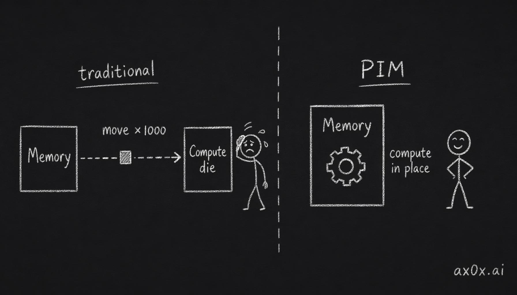 Processing-in-memory puts arithmetic units inside the memory itself, so the bytes never make the expensive trip across the bus that costs ~1000x the compute.
The concrete claims are tantalizing. Vendor demos — SK Hynix's AiM line on memory-bound GEMV (the matrix-vector work that dominates LLM decode), Samsung's HBM-PIM on attention-heavy kernels — claim "dozens of times" better energy efficiency on exactly the memory-bound operations that bottleneck inference. Those are the kinds of gains that, if they held at scale, would move the whole efficiency frontier.
But that "if" is the whole story, and PIM is the longest-dated of all five. As of early 2026 it's still substantially prototype-and-patent for production inference. There's a real on-ramp now — HBM4's logic base die is a place to eventually put compute, and LPDDR6-PIM standardization is just starting — but "biggest theoretical payoff, furthest from your data center" is the right summary. PIM is the answer if the wall is permanent. It is not the answer to the wall in front of us this year.
HBF is the one that genuinely surprised me
Now the one that ties this whole series back to NAND, and the one I think is underrated.
SanDisk's pitch with HBF — High Bandwidth Flash — starts from a question that sounds almost dumb: if a huge part of inference is reading (model weights, retrieved documents, cold context) and barely writing, why are we paying for DRAM at all? DRAM's whole expensive premium is fast, infinite rewrites. Inference of static weights doesn't need that. So SanDisk stacks NAND the way HBM stacks DRAM — TSVs, base logic die, the works — and gets a part with roughly 8–16x the capacity of HBM (a 512 GB, 16-die stack against HBM4's ~48 GB) at, per SanDisk, comparable system cost.
Read that carefully, because the easy version is wrong. SanDisk does not say HBF is cheaper than HBM; they say comparable cost for far more capacity — better cost per gigabyte. And it is not shipping: pre-production samples are targeted for the second half of 2026, devices around early 2027. The limits are exactly NAND's limits from post 3 — microsecond-class latency (10–100x slower than DRAM), page-granular reads, and write endurance around 10^5 cycles. That endurance ceiling is decisive: HBF is for read-heavy weights you load once and hammer, not for per-token KV-cache that you rewrite constantly. Used in its lane, the numbers are real — within ~2.2% of an unlimited-HBM baseline on Llama 3.1 405B weight reads.
The most interesting move isn't HBF alone, it's the hybrid. SK Hynix signed an MOU with SanDisk in August 2025 to put HBM and HBF on the same interposer — fast HBM for the writes, vast HBF for the read-only weights — so a single package holds both the speed and the capacity. That's not routing around the wall. That's building a taller, cheaper section of it out of flash. And it's the fourth direction, after CMX, that ends with NAND doing inference work it was never built for.
Which is why NAND stopped being cold storage
Step back and the four workarounds rhyme. CMX tiers KV-cache to NAND. HBF stacks NAND like HBM. Checkpointing dumps trillion-parameter training state to NAND. RAG and vector stores read embeddings off NAND in the serving path. The chip that, for thirty years, was where data went to wait is now in the hot loop of AI from every angle.
The receipts are in the revenue, and they're not subtle. Per TrendForce, top-5 enterprise SSD revenue went +28% QoQ in Q3 2025 and +51.7% in Q4 — and top-5 NAND revenue then jumped +83.7% QoQ to $38.9 billion in Q1 2026. A 30TB enterprise SSD that ran ~$3,062 in April 2025 was ~$9,318–11,000 by Q1 2026. The 2026 NAND market is forecast at $270.6 billion, up ~280% year over year. The reason "your SSD got expensive" rhymes with "HBM got expensive" is that they're now the same demand curve — AI is buying both ends of the pyramid at once. NAND is no longer the cheap floor of the stack. It's an inference-grade tier with inference-grade pricing.
Meanwhile China is climbing the wall from below
Every workaround above is the West routing around the wall at the top. China is doing something different: building the wall from the bottom, brick by brick, under sanctions.
On NAND, YMTC is already there at scale. It holds roughly 11.8–13% of the global NAND market — most of it sold domestically — on a 294-layer Xtacking process, running around 200k wafers per month with ~45% domestic-tool adoption. It has been on the US Entity List since December 2022 and grew its share through it. YMTC filed for IPO tutoring on May 19, 2026, reportedly targeting a $30 billion-plus raise. For the cheap, high-volume layer of the stack, China is no longer climbing — it's standing on the wall.
On DRAM, CXMT is climbing fast and not yet at the top. On a 16nm G4 process it's shipping DDR5-8000 and LPDDR5X-10667, and it took 7.67% of the global DRAM market in Q4 2025. The growth numbers are almost comical — Q1 2026 revenue of RMB 50.8 billion, up 719% year over year, on roughly RMB 25 billion of net profit. Its STAR Market IPO was approved by the listing committee on May 27, 2026, at RMB 29.5 billion ($4.4 billion), the second-largest in that exchange's history. Xiaomi is reported to hold a stake via the Hubei Xiaomi Changjiang fund — though I'd flag that the popular "to lock up supply" reading is interpretation, not a stated motive; Xiaomi is also a customer.
But here's the honest caveat, and it's the one that matters for timing: CXMT's HBM is sampling, not shipping. It has sent HBM3 samples to Huawei. Volume is realistically a 2027–28 story, not a 2026 one. So the China narrative splits cleanly: a real, sanctions-proof NAND business today, and an HBM ambition that's directionally inevitable but two-plus years from moving the global supply needle. Anyone telling you Chinese HBM relieves the 2026 shortage is selling you a 2028 fact dated to this year.
So when does the cycle actually turn?
This is the only question readers actually want answered, so let me answer it the way I'd answer it on the Compute Labs side of my desk, where the timing of a memory glut is not academic.
What ends a memory cycle is never demand softening — AI demand is the most non-discretionary capex on earth right now. What ends it is supply catching up while demand digests: enough new HBM bit-supply, enough new CoWoS packaging capacity, enough fab output to flip deficit to surplus, arriving at the same moment hyperscaler buying pauses to absorb what it already bought. That's the mechanism that broke 2019 and 2022, every time.
Now line up everything in this post against that mechanism. CMX, CXL, Cerebras, PIM, HBF, Chinese HBM — none of them adds meaningful HBM-grade supply in 2026. The workarounds reduce the need for HBM at the margin and shift load to NAND; they don't flood the market with the constrained part. Chinese HBM is a 2027–28 event. And the part everyone forgets is that HBM bit-supply isn't even the binding constraint — packaging is. An HBM stack is useless until it's sat on an interposer next to the logic die, and that step is TSMC's CoWoS line, which is sold out. TSMC is ramping CoWoS from roughly 75–80k wafers per month at the end of 2025 toward a 120k-plus target by the end of 2026 — a real, large addition, and still not enough to flip the market, because demand is climbing the same curve. The supply side does not break the wall this year.
That is the whole conclusion, stated cleanly: because supply won't break the wall in 2026, the turn in this cycle will not come from supply in 2026. If it comes, it comes from the demand side — a hyperscaler capex pause, double-ordering unwinding, an AI-spending wobble — and that's a different, faster, more brutal kind of turn than a slow supply glut. The analysts cluster the acceleration peak around Q3–Q4 2026, with absolute prices staying elevated through 2027 and no return to 2024/25 pricing before 2028 (IDC, Counterpoint's Q4 2027 inflection, DBS's late-2027 call, Intel's Lip-Bu Tan flatly saying "no relief until 2028"). My read tracks theirs: the rate of acceleration cools in the back half of this year, prices stay high through 2027, and the genuine glut risk — the one the bears are right to watch and the bulls wrong to dismiss — is a 2028 event, gated by when the new fabs and CoWoS lines and Chinese HBM all land at once.
What I'd actually watch, in order: HBM bit-supply growth guidance from the three makers, TSMC's CoWoS capacity additions through 2026, and hyperscaler capex guidance — because the first crack will show up as a capex sentence on an earnings call, not as a price print. As long as Jensen's customers keep raising capex and CoWoS stays sold out, the wall holds and the cycle runs.
The wall moved, and so did the money
I opened this series by complicating a thing I'd written before — that all AI problems reduce to compute. They do. But the binding constraint inside compute moved. For two decades it was FLOPS; now it's the bandwidth and capacity of the memory sitting next to the logic. That's not a footnote. It's why three memory makers crossed a trillion dollars within weeks of each other, why SanDisk is restacking flash, why Google argues against its own pooling tech, why China is racing two IPOs to the wall, and why the thesis I actually bet on is the unglamorous layer underneath the models — the silicon and the systems, and now, specifically, the memory.
Every workaround in this post is someone who saw the wall clearly and moved early. That's the only edge there is in this business. The wall doesn't reward the people who climb it. It rewards the people who priced it first.


