How DRAM Works — and Why It Got Scarce
 A single DRAM cell drawn as a leaky bucket — one transistor, one capacitor, charge draining out, being refilled thousands of times a second
If you tried to build a PC or upgrade a phone in the back half of 2025, you already felt this post before you read it. A DDR5 kit that cost a certain amount in early 2025 cost two to three times that by year-end — spot prices on some 16Gb DDR5 chips ran from about $6.84 in September to $27.20 in December. That's nearly a 300% jump in three months, per spot-market data tracked by TrendForce. Phone makers started warning that next year's models would cost more, or quietly shipped less RAM in the same chassis. The thing getting more expensive was not the processor. It was the memory.
In the last post I argued that the bottleneck inside a modern AI accelerator stopped being raw FLOPS years ago — it's memory bandwidth and capacity. I finance the machines AI runs on, and the line item that surprises people most when they see a server bill is how much of it is just memory. So this post goes down one level: what is DRAM, physically, and why is something we've been mass-producing since the 1970s suddenly the scarce, expensive thing?
The answer starts with a bucket that leaks.
DRAM remembers by holding a charge that's always draining away
The basic unit of DRAM — the thing that stores one bit — is almost insultingly simple. It's one transistor and one capacitor. Engineers call it 1T1C. The capacitor holds an electric charge: charged means 1, empty means 0. The transistor is a gate that lets you read or write that charge.
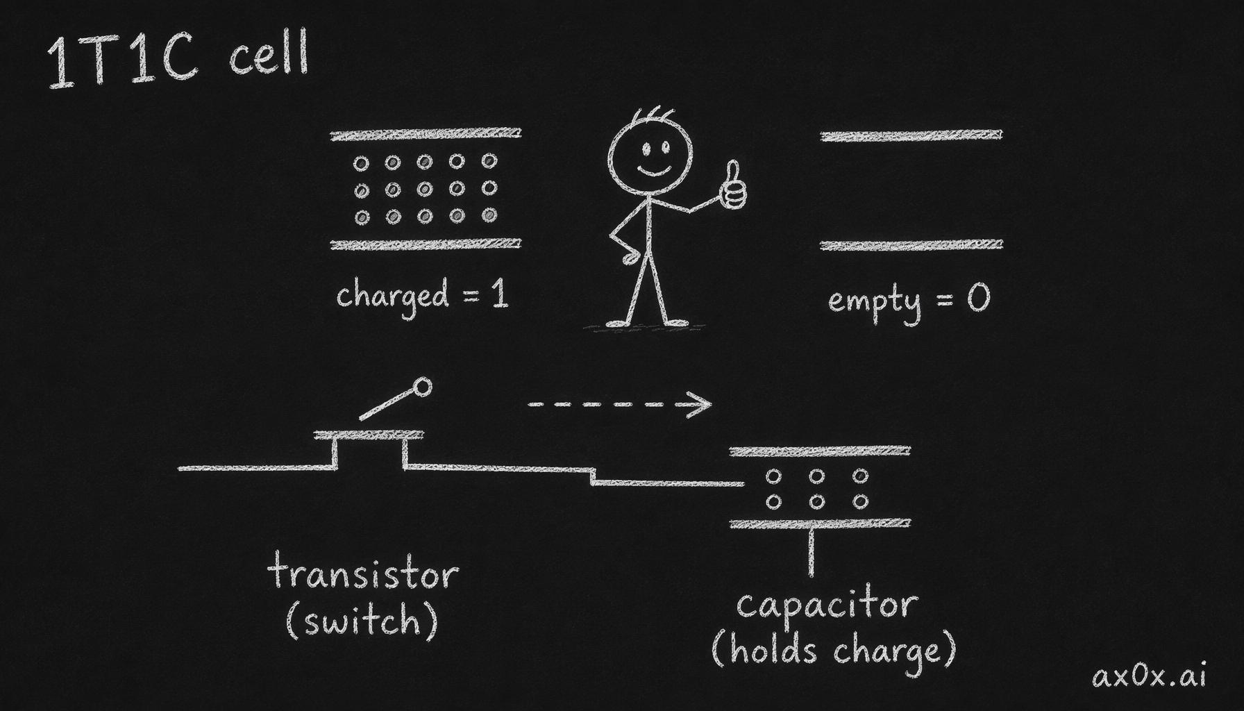 One DRAM cell: a transistor acts as the switch, a capacitor holds the charge — charged is 1, empty is 0
That's it. That's the whole memory cell. SRAM — the fast memory inside the CPU's caches — needs six transistors to store the same single bit. The fact that DRAM does it with one transistor and a capacitor is exactly why DRAM is cheap and dense enough to give you 32GB in a stick, while SRAM caps out at tens of megabytes on a whole processor.
But the capacitor has a fatal flaw: it leaks. The charge bleeds away on its own in tens of milliseconds. Leave a DRAM cell alone for a fraction of a second and the 1 quietly decays into a 0 — the memory forgets.
The fix is brute force. The chip reads every single cell and writes the value back, over and over, before the charge can drain — every 32 to 64 milliseconds, depending on the part. That constant rewrite is called refresh, and it's where the D in DRAM comes from: dynamic means the data is never sitting still, it's being continuously regenerated. On an advanced node a single cell's capacitor holds under one femtofarad of charge (about 0.7 fF), an almost unimaginably tiny amount — which is why it drains so fast and has to be topped up so often.
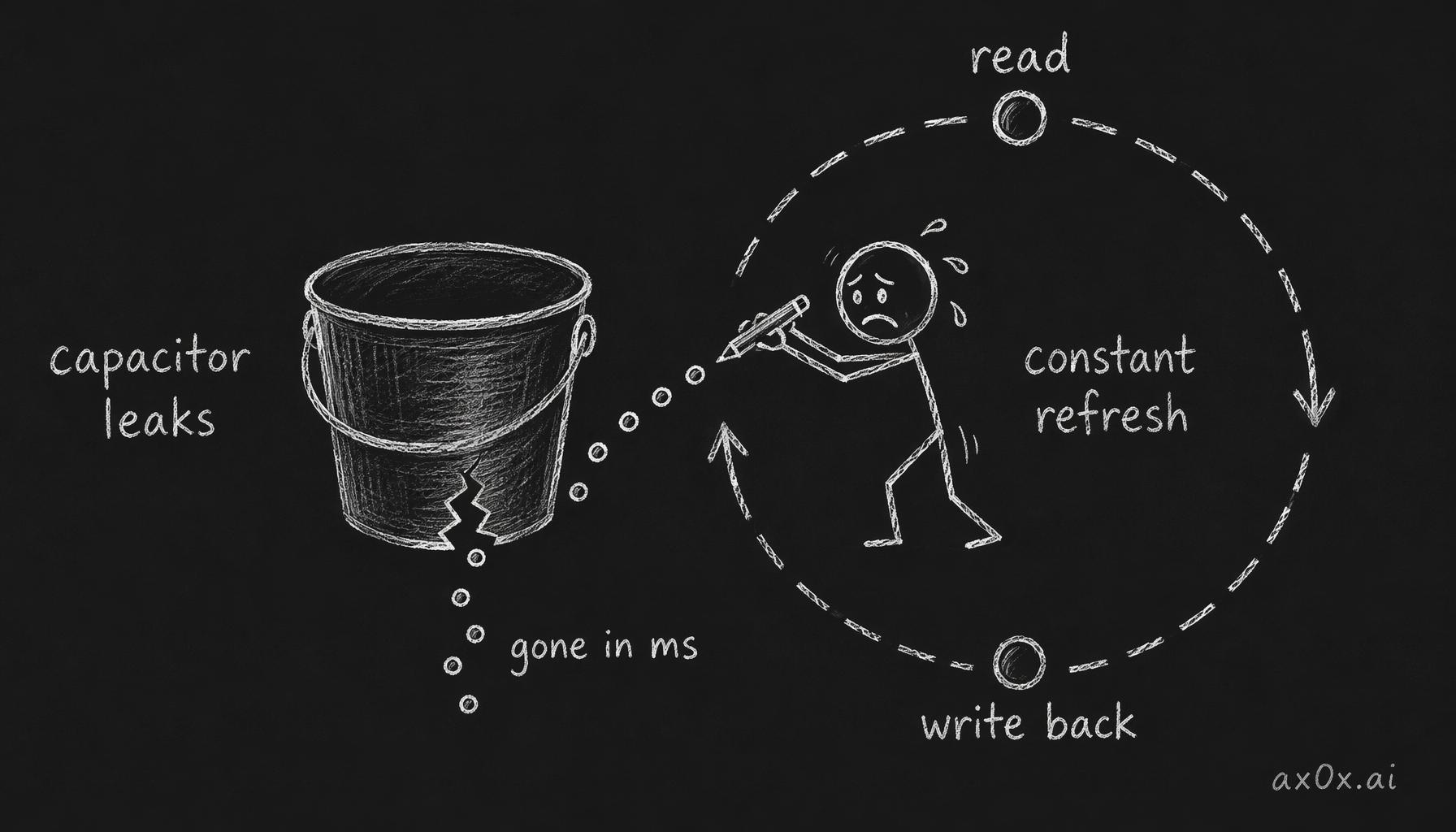 A DRAM capacitor is a leaky bucket — the charge drains in milliseconds, so the chip must read every cell and write it back, forever
Refresh isn't free. Constantly rewriting billions of cells burns power even when the chip is doing no useful work — on dense modern parts, refresh can eat north of 10% of the DRAM's total power budget, per SemiAnalysis's teardown of memory physics. And it's why DRAM is volatile: cut the power and refresh stops, the charge drains, and everything is gone in well under a second. Your RAM forgets the instant you pull the plug. That's not a bug — it's the direct consequence of storing data as a charge in a leaky bucket.
So hold onto this one image, because the rest of the story falls out of it: DRAM is fast because the cell is dumb and tiny, and it's volatile and power-hungry because that same tiny cell can't hold its charge for more than a few hundredths of a second. Speed, volatility, and the refresh tax are all the same physical fact wearing three hats.
The DDR ladder is just the same cell going faster every few years
Once you understand the cell, the alphabet soup on a spec sheet — DDR4, DDR5, LPDDR5X, GDDR7 — stops being intimidating. They're all the same 1T1C cell. What changes between them is how you talk to it: the interface, the voltage, the width, the clocking. Each generation is mostly a bandwidth-doubling exercise wrapped around an identical leaky bucket.
DDR4 is what most computers ran for the last decade. It launched in 2014, runs at 1.2 volts, and the JEDEC spec tops out around 3,200 MT/s (mega-transfers per second), which is roughly 25.6 GB/s per module. Solid, boring, everywhere.
DDR5 is the current generation, standardized in mid-2020, with SK Hynix shipping the first production chip in October that year. It dropped the voltage to 1.1V, split each DIMM into two independent 32-bit sub-channels, put a small power-management chip and on-die error correction onto the module itself, and runs from 4,800 MT/s up to 8,800 MT/s in the JEDEC spec — with enthusiast kits pushing past 9,600 by 2025. Net result: roughly double the bandwidth of DDR4.
One myth worth killing: people assume each new generation is "faster" in every sense. It isn't. DDR5's raw latency — the time to fetch one specific byte — is actually no better, sometimes slightly worse, than well-tuned DDR4. What DDR5 buys you is throughput: more bytes per second moving in parallel. For an AI workload that's streaming gigabytes of model weights, throughput is everything and single-access latency barely matters. That distinction — bandwidth versus latency — is the whole reason the memory wall exists, and it's the thread running through this entire series.
Two cousins matter for context:
LPDDR is the low-power branch — the RAM in your phone. LPDDR5 hit 6.4 Gbps per pin, LPDDR5X pushed to about 10.67 Gbps, and LPDDR6 was standardized in mid-2025 at 14.4 Gbps with wider channels. The interesting move is that LPDDR is creeping out of phones and into AI servers: Nvidia's Grace-class CPU parts use LPDDR precisely because, per unit of bandwidth, it sips power compared to server DDR5 — and in a rack where every watt is contested, that matters.
It's worth sitting with why that swap happens at all, because it tells you how the economics of an AI data center have inverted. For decades, low-power memory was a compromise you made for battery life and accepted a performance hit for. In a phone, the constraint is the milliamp-hours in your pocket. In a rack of AI accelerators, the constraint is the same — except the "battery" is the power and cooling envelope of the building, and it is just as finite. A modern training rack can pull tens of kilowatts, and a large chunk of that never touches a math unit; it goes to moving data and keeping memory alive. So when a CPU part can serve its memory at the same bandwidth for meaningfully fewer watts, that saved power doesn't vanish — it gets redirected into more GPUs, more interconnect, more useful compute under the same fixed ceiling. The phone's design constraint and the data center's design constraint turned out to be the same constraint, just scaled up by six orders of magnitude. That's why a memory type born to make laptops thin is now showing up next to the most expensive silicon on Earth.
GDDR is the graphics branch — the RAM soldered next to a gaming GPU. It trades capacity and flexibility for ferocious per-pin speed. GDDR7, which JEDEC finalized in 2024 and went into mass production in 2025, uses three-level signaling (PAM-3) to hit up to 48 Gbps per pin. An RTX 5090 pairs GDDR7 at 28 Gbps across a 512-bit bus for about 1,792 GB/s — a 78% jump over the previous flagship. Hold that "wide bus = huge bandwidth" idea: it's the seed of how HBM works, which is the next post.
Same cell. Different conversation with it. That's the whole ladder.
DDR4 was supposed to die in 2025 — instead it sold above DDR5
Here's where the physics meets the market, and where the price spike you felt comes from.
By early 2025, DDR4 was a decade-old technology. The plan, as you'd expect, was to wind it down. Micron issued formal end-of-life notices on DDR4 parts around June 2025, and the Big Three memory makers (Samsung, SK Hynix, Micron) all signaled they'd shift their fab capacity off legacy DDR4 and toward the products that actually make money now — DDR5 and HBM. Old node, retire it, move on. Standard industry housekeeping.
Then two things happened that broke the script.
First, the trigger most people get wrong. The initial DDR4 price spike, around March 2025, wasn't caused by the Big Three's wind-down at all. It was caused by China's CXMT — the rising mainland DRAM maker — pivoting its output off DDR4 toward newer products, which yanked a big chunk of cheap DDR4 supply out of the market in one move. Jim Handy, the analyst who writes as The Memory Guy, traced the early spike to exactly this. DDR4 8Gb spot prices jumped about 56% in May 2025 alone, from roughly $1.75 to $2.73.
Second, and this is the genuinely strange part: the price kept climbing until DDR4 cost more than DDR5. By around July 2025 there was a price inversion — the old, slower, decade-old chip was selling above the new, faster one. That is not supposed to happen. New tech is supposed to be expensive and old tech cheap; that's the whole shape of the semiconductor business.
What broke it was the wall I keep coming back to. HBM and DDR5 demand from AI servers had swallowed so much fab capacity that nobody wanted to keep cranking out low-margin DDR4 — but the installed world still needed it. Every data center running older servers, every industrial controller, every networking box, every appliance with a years-long design cycle suddenly faced a last-time-buy panic: stock up now or get stranded. Buyers hoarded, supply was being deliberately starved, and the price of a "dead" product went vertical.
So Samsung and SK Hynix did the rational thing — they reversed course and extended DDR4 production into 2026 to harvest the shortage they'd helped create. (This is the precise version, and it matters: they didn't "kill DDR4 production," as a lot of headlines claimed. They signaled retirement, the market panicked, and they walked it back to keep selling into the panic.) Old technology, priced above new technology, kept alive specifically because it became briefly more profitable than the cutting edge. That single inversion tells you everything about how distorted the memory market got in 2025 — and it's the on-ramp to the supercycle this series builds toward.
The reason DRAM can't just make more is a capacitor that refuses to shrink
A reasonable person asks: if memory is this scarce and this profitable, why don't the makers just shrink the chips, fit more bits per wafer, and flood the market? That's what's worked for fifty years — Moore's Law, smaller transistors, more for less.
DRAM stopped getting that deal a while ago, and the culprit is the same leaky capacitor from the top of this post.
For logic chips — the processors — "nodes" march down through real nanometer numbers: 5nm, 3nm, 2nm. DRAM has been stuck in what the industry calls the 10nm class since roughly 2018, labeling generations not with numbers but with Greek letters: 1x, 1y, 1z, then 1α, 1β, and now 1γ (one-gamma). Micron shipped 1γ DDR5 samples in early 2025 — about 30% more bit density, over 20% lower power, 15% better performance than the prior 1β node. Real progress, but incremental, and the steps are getting smaller and slower.
The bottleneck is the capacitor. To store a reliable, readable charge in a cell, the capacitor needs a certain minimum capacitance — and capacitance scales with surface area. As the cell footprint shrinks, the only way to keep enough surface area is to build the capacitor up: a tall, impossibly narrow cylinder or trench. Modern DRAM capacitors run aspect ratios past 50-to-1 — picture a drinking straw the height of a skyscraper, etched into silicon billions of times over, each one identical. Shrink the footprint further and the straw has to get taller and thinner to hold the same charge, until it physically can't stand up. That's the wall, and it's mechanical, not just lithographic.
It helps to picture what failure looks like at that aspect ratio, because the wall isn't an abstraction — it shows up as yield. When you etch billions of holes this deep and this narrow, every one of them has to come out straight, the same depth, and clean to the bottom. A few that bow, taper, or collapse against a neighbor aren't a rounding error; each is a dead bit, and a die has billions of them. Push the geometry past where the etch is reliable and the defect rate climbs faster than the density you gained, so a "smaller" cell that should fit more bits per wafer can actually yield fewer good ones. That's the cruel part of this particular wall: it doesn't announce itself as a hard stop. It shows up first as a node that's technically manufacturable but economically pointless — you can make it, you just can't make money on it — which is exactly why the cadence of new DRAM generations has stretched from two years to three and beyond.
Making these structures now requires EUV — extreme ultraviolet lithography, the most expensive tooling in the industry. EUV buys a few more nodes; it doesn't repeal the geometry problem.
Two escape hatches are on the roadmap, both hard:
- 4F² cell layout. Today's DRAM cell has used a 6F² layout since around 2007 (F is the smallest printable feature). Moving to 4F² would cut cell area by about a third — SK Hynix demonstrated a 4F² "Vertical Gate" structure at the 2025 VLSI symposium. But it buys maybe three more nodes, not an open-ended runway.
- 3D DRAM. The real escape is to do to DRAM what the industry already did to flash: stop shrinking sideways and start stacking vertically. NAND solved its own scaling wall this way years ago — which is the next post's whole story. But 3D DRAM is genuinely hard — you have to stack the capacitor itself, not just wiring — and mass production isn't expected until somewhere in the early 2030s. It also leans on older DUV lithography rather than EUV, which raises the awkward possibility that the EUV tools makers are buying today become stranded assets within a decade.
Put it together and the supply side of the price spike makes physical sense. DRAM can't conjure dramatically more bits per wafer the way it used to — the capacitor won't shrink, 4F² buys a little time, and the real fix is a decade out and needs a nearly new playbook. So when AI demand hit, supply couldn't elastically respond. Scarcity wasn't a choice. It was geometry.
DRAM is the substrate everything else is built from
Step back and the whole post is one idea seen from different angles. A bit of DRAM is a charge in a leaky bucket. Because the bucket is tiny and dumb, DRAM is dense and cheap — but because it leaks, DRAM is volatile, power-hungry, and refreshed thousands of times a second. Because the capacitor that forms the bucket refuses to shrink, the whole category hit a scaling wall right as AI demand went vertical. And because old DDR4 got starved of fab capacity, a decade-old chip ended up priced above its successor.
But the most important thing about DRAM isn't in your laptop. It's that DRAM is the raw material for the most contested component in the AI economy. HBM — the high-bandwidth memory stacked next to every AI GPU, the part that's roughly half the cost of the chip itself — is not some exotic new memory. It's ordinary DRAM dies, thinned out and stacked vertically and wired together by the thousands. Every limitation in this post — the leaky cell, the refresh tax, the capacitor that won't shrink — HBM inherits all of it, and then adds a stack of new problems on top.
Which is why the next chip you can't buy and the next stock that just hit a trillion dollars both trace back to the same leaky bucket. Understand the bucket, and the rest of the memory stack is just engineering on top of it.


